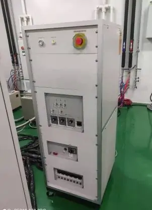
The Hitachi S-8840 is a high-precision CD-SEM dedicated to critical dimension measurement for semiconductor wafers. Utilizing high-resolution electron optics, it captures detailed top-down images and measures fine pattern geometry for process control in etch and lithography steps.
Fitted with stable beam control and automated recipe setup, it delivers consistent, repeatable CD readings. It detects tiny pattern deviations and profile anomalies, supporting daily inline inspection inside cleanroom environments.
Built for long-hour continuous production, this system offers reliable performance and manageable maintenance. It easily fits into your existing fab workflow to monitor pattern quality and secure final product yield.

Hitachi S-8840 Main Specifications
| Manufacturer | Hitachi |
|---|---|
| Model | S-8840 |
| Equipment Type | Critical-Dimension Scanning Electron Microscope |
| Supported Wafer Sizes | 150 mm and 200 mm |
| Compatible Wafer Thickness | Approximately 0.4–1.0 mm, according to the available listing |
| Wafer Cassette Capacity | 25 wafers per cassette |
| Published Image Resolution | 5 nm |
| CD Measurement Range | 0.1–10 µm |
| CD Repeatability | 3σ ≤5 nm or ≤±1% |
| SEM Magnification | 1,000× to 150,000× |
| Optical Microscope Magnification | Approximately 110× |
| Wafer Handling | Cassette-to-cassette automatic wafer transfer and alignment |
| Condition | Used semiconductor equipment |
| Availability | Subject to current stock, inspection and configuration confirmation |