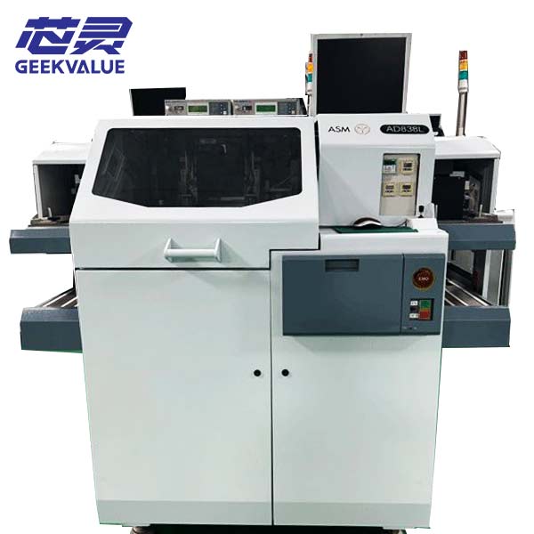
ASMPT AD838L Automatic Die Bonder
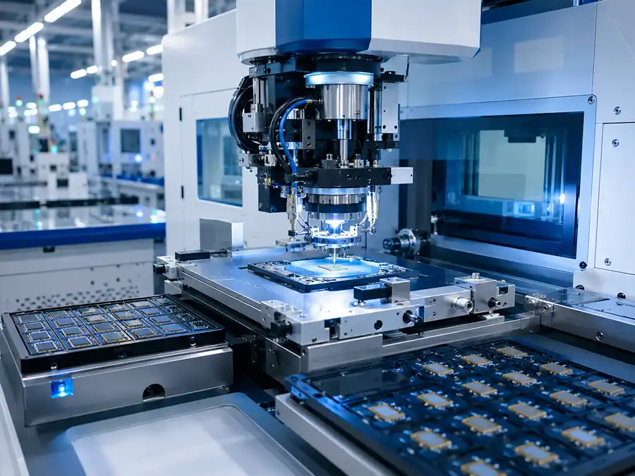
ASMPT AD838L automatic die bonder. ±10 μm @ 3σ (±15 μm with up-look), ~14,000 UPH. Dies 0.15–2.03 mm, substrates up to 300 × 100 mm. Up-look PR, flip chip, dual dispense.
Review Equipment Details
GK-SEMI supports semiconductor manufacturers, OSAT facilities and equipment teams with process equipment, machine configuration review, spare parts sourcing and technical coordination—from wafer preparation and die attach to package testing and finalization.
Start with device, process, output and integration requirements.
Confirm model, options, tooling, software and included items.
Inspection scope is matched to new, used or refurbished equipment.
Parts, technical coordination and replacement planning after delivery.
Move from a machine name to the actual production requirement. Explore equipment categories for wafer processing, precision assembly, IC testing, package finalization and process support.
Assembly and bonding equipment places and connects semiconductor die to packages. This category covers die bonders (epoxy, eutectic, sinter), wire bonders (gold, copper, aluminum), and flip chip bonders (TCB, mass reflow). Selection depends on die size, substrate, interconnect metallurgy, and production volume.
View Equipment Category
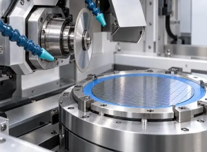
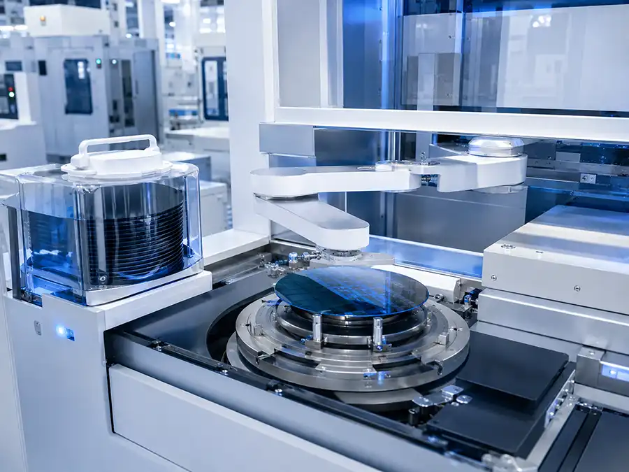
Wafer processing equipment prepares semiconductor wafers for singulation and packaging. It includes wafer mounters (dicing tape, BG tape), grinders (backgrinding, TAIKO), cleaners (post-dicing, post-CMP), and dicing saws (blade, laser). The correct sequence depends on wafer thickness, material, and downstream packaging.
View Equipment Category
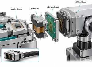
Semiconductor test equipment verifies device functionality and performance. This category includes ATE systems (SoC, mixed-signal, PMIC), test handlers (pick-and-place, gravity, turret), and probe stations (manual, semi-automatic, automatic). Key selection factors are tester interface, site count, temperature range, and package format.
View Equipment Category
Packaging and finalization equipment encapsulates and finishes semiconductor packages. It covers molding machines (transfer, compression), trim and form systems, and laser marking machines. Critical factors include mold chase compatibility, leadframe handling, marking contrast, and traceability requirements.
View Equipment Category
Process support equipment ensures stable surface and material conditions for critical steps. This category includes plasma cleaners (O₂, Ar chemistry) for adhesion promotion and electroplating systems (Cu, Ni, Au) for metal deposition. Matching chamber geometry, gas chemistry, and chemistry compatibility to the process is essential.
View Equipment CategoryEquipment should be evaluated as part of a connected production route. Upstream material condition, placement accuracy, interconnect method and test requirements all influence the correct machine configuration.
Cleaning, mounting, thinning and dicing before die-level assembly.
02 / PLACEDie bonding and flip chip placement for the required package structure.
03 / CONNECTWire bonding and advanced interconnect according to pitch and material.
04 / PROTECTMolding, trim and form, marking and surface finishing operations.
05 / VERIFYProbe, electrical test, thermal handling, sorting and final verification.
Browse selected semiconductor equipment listings. Availability, installed options, condition and delivery scope should be confirmed for each individual machine.
ASMPT AD838L automatic die bonder. ±10 μm @ 3σ (±15 μm with up-look), ~14,000 UPH. Dies 0.15–2.03 mm, substrates up to 300 × 100 mm. Up-look PR, flip chip, dual dispense.
Review Equipment Details
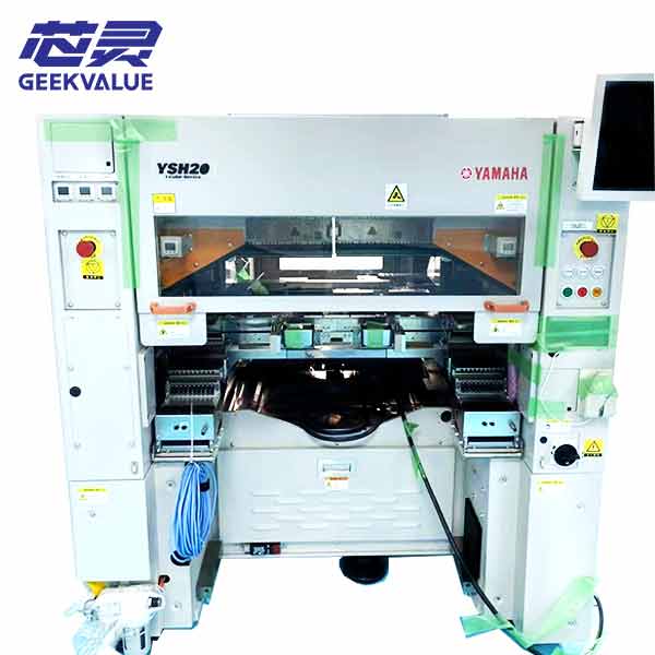
Used Yamaha YSH20 hybrid flip-chip placer with ±10 μm accuracy, 4,500 UPH, and 6/8/12-inch wafer support. Bump inspection and SMT-compatible handling. Request a quote.
Review Equipment Details
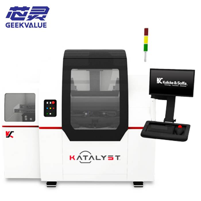
K&S Katalyst flip chip die bonder, 3 μm placement accuracy, 15,000 UPH instantaneous throughput, dual-bond head with 12 nozzles, for Micro LED assembly bonding, compatible with AGV/OHT a...
Review Equipment Details
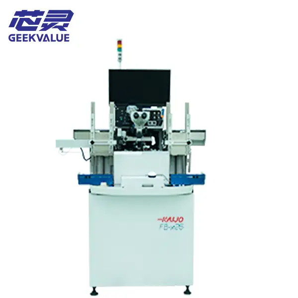
KAIJO FB-x26 wire bonder for high-volume IC assembly: 95mm Y-axis range, 3σ ≤ 3.0μm accuracy, Au/Cu/Ag wire, SECS/GEM ready. See specs and application fit.
Review Equipment Details
KAIJO FB-i28 high-precision wire bonder: ±2.0μm accuracy, 35μm pad pitch, low-impact bonding for low-k and stacked die. See full specs and application fit.
Review Equipment Details
Thermosonic ball/wedge bonder, 3σ ≤ 2.0 μm, 43 ms per wire. Gold, copper, silver alloy wire. α eyes vision, dual-frequency transducer.
Review Equipment DetailsSolution pages connect equipment categories to practical manufacturing requirements, helping project teams identify the process variables that matter before requesting a machine.
Die attach, wire bonding and interconnect equipment for package assembly.
→ SOLUTION 02Coordinate device handling, tester interface, temperature and throughput.
→ SOLUTION 03Package protection, forming, marking and surface finishing routes.
→ SOLUTION 04Cleaning, thinning, mounting and singulation before assembly.
→ SOLUTION 05Fine-pitch, multi-die, flip chip and heterogeneous integration pathways.
→A model number is only the beginning. A useful proposal should define the application, equipment configuration, condition evidence and delivery scope before commercial comparison.
Start an Equipment ReviewDevice or wafer type, package architecture, substrate, target accuracy, throughput, temperature range and integration constraints.
Review model generation, installed options, handling format, tooling, software version, utilities and line compatibility.
Define the inspection scope, running evidence, critical assemblies, included accessories and acceptance requirements.
Align packing, export documentation, installation expectations, training, spare parts and post-delivery support.
Three supply routes: As-Is, Inspected & Serviced, and Fully Refurbished.Each unit ships with a condition report, tooling list and software version record. Site requirements confirmed before shipment.
Explore Available EquipmentBonding tools, dispenser valves, heater blocks, vacuum sensors, servo drives and PR cameras. Send the part number and photos; we confirm repair or replacement route with lead time.
Explore Parts & Support
Semiconductor equipment projects depend on configuration details, process fit and long-term support. We help global production and engineering teams evaluate equipment, parts and service requirements with a clearer technical and commercial scope.
Send the equipment model, application, required configuration, preferred condition, quantity and destination country. Our team will review the most practical equipment or support route for your project.