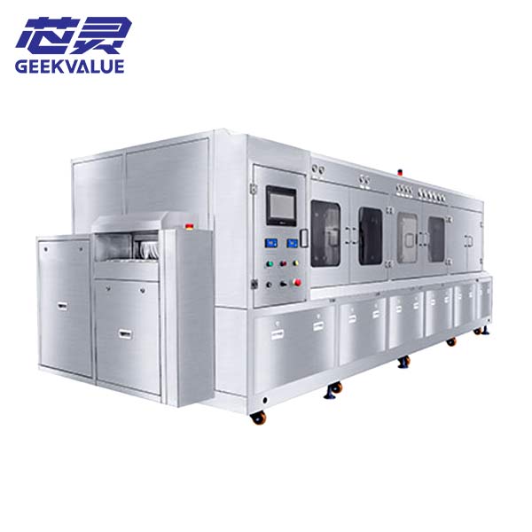
Semiconductor Package Cleaning Machine SC810
Semiconductor package flux cleaner. Gets rid of rosin, water-soluble, and no-clean flux after soldering. Takes BGA, CSP,...
We stock used wafer cleaners from TEL, SCREEN, SEMES, LAM Research and other platforms — post-dicing scrubbers, post-CMP cleaners, single-wafer wet systems and flux removal tools. The unit that fits your line depends on four things: the contamination type, the wafer condition, the cleaning method and the downstream process. Most used-wafer-cleaner purchases that go wrong fail at one of these four points. Tell us your requirements and we'll shortlist the systems that actually work on your line.
Two wafer cleaners with the same model name can have very different capabilities. The installed brush type, nozzle configuration, chemistry compatibility, chuck and handling system matter more than the platform name alone. Review the current inventory, then send us your contamination and process requirements for a configuration check.
Looking for a specific TEL, SCREEN, SEMES, LAM Research or other wafer cleaner? Send the model number even when it is not currently shown — our sourcing team will check availability.
Semiconductor package flux cleaner. Gets rid of rosin, water-soluble, and no-clean flux after soldering. Takes BGA, CSP,...
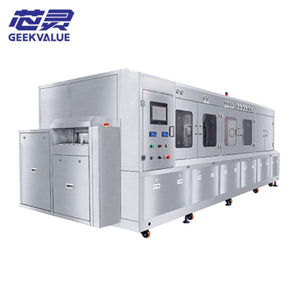
Micro LED/Mini LED inline washer. Heated DI spray lifts water-soluble flux and residue. High-flow rinse reaches under th...
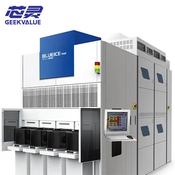
Fully automatic 300mm single-wafer cleaner. High-temp phosphoric acid process, 19nm particle removal. Proprietary high-t...
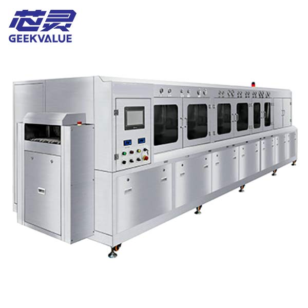
Inline plasma cleaner. Strips flux and organic/inorganic residue after soldering. Runs lead frames and IGBTs. Temp and l...
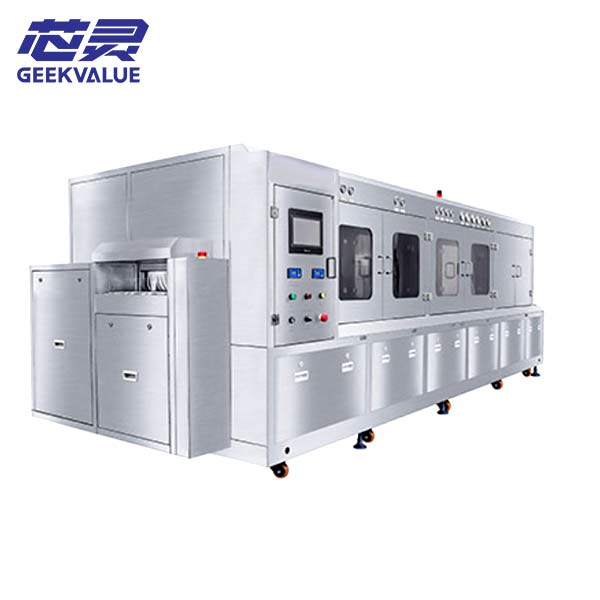
Automatic inline chip cleaner. Multi-mode aqueous cleaning. One-button start, enclosed design. Ultrapure water, no harsh...
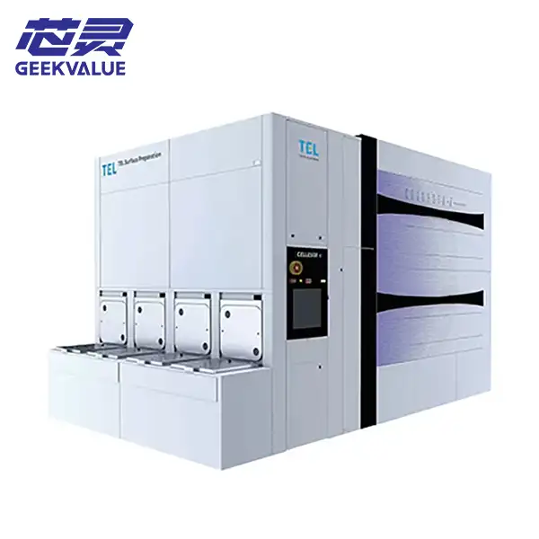
300mm single-wafer cleaner, 10nm and below. No damage, chamber atmosphere control, better IPA dispense so patterns don&#...
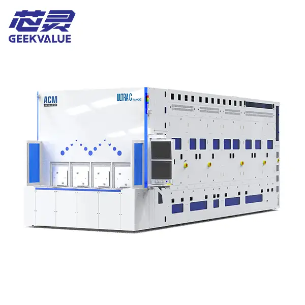
Up to 12 process chambers, 800 WPH. APAC atmosphere control for 22nm and below. Handles 32nm to 7nm nodes, plus SiC and ...
We've seen buyers order a "wafer cleaner" expecting a post-CMP scrubber, then discover the unit is configured for post-dicing debris removal — the two use different brush types, nozzle configurations and handling systems. Identify what is on the wafer and what process comes next before comparing brands, automation levels or machine specifications.
Particles and debris generated during dicing. Requires brush scrubbing, spray cleaning or megasonic rinse with edge handling to avoid damage.
Slurry particles and polishing residue after chemical mechanical planarization. Typically requires double-sided PVA brush scrubbing and megasonic assistance.
Flux and solder residue after packaging or soldering. Requires spray cleaning with DI water and compatible chemistry, often with heated stages.
Organic films, metallic contamination or particles from handling. May require wet bench processing, chemical cleaning or plasma-based methods.
Scrubber, spray, single-wafer wet, batch wet or megasonic. The method must match the contamination type, wafer surface and cleanliness target.
Sales shortcut: tell us what is on the wafer and what process comes next. We can then narrow the cleaning method, chemistry compatibility and automation level without making you specify every component first.
“Wafer cleaner” is a broad equipment category. A system for standard silicon wafers is not automatically suitable for ultra-thin, bumped, MEMS or compound semiconductor substrates.
Conventional wafers where standard brush scrubbing or spray cleaning can remove particles without surface damage.
Thin wafers and TAIKO profiles require special support, reduced pressure and controlled edge handling to prevent breakage.
Bumps, MEMS structures, backside features or fragile surfaces can require non-contact cleaning and dedicated recipes.
Wide-bandgap and compound substrates may require different chemistry, handling and damage limits compared to silicon.
Glass carriers, panels and substrates require flatness control, gentle handling and compatible cleaning chemistry.
Packaged devices and substrates after soldering require flux residue removal with spray or immersion cleaning.
The cleaning method must match the contamination type, wafer surface and cleanliness target. Each method has different strengths and limitations.
| Decision Point | Brush Scrubber | Spray Cleaner | Single-Wafer Wet | Batch Wet Bench |
|---|---|---|---|---|
| Typical Use | Post-CMP and post-dicing particle removal on standard wafers. | Flux residue removal and package cleaning after soldering. | Advanced 200mm/300mm cleaning with multiple chemistries. | Batch processing for high-volume particle and organic removal. |
| Cleaning Action | PVA brush scrubbing, often double-sided, with optional megasonic rinse. | High-pressure DI water spray with optional chemistry and heated stage. | Spin cleaning with chemical dispense, rinse and dry in one chamber. | Immersion or spray in a wet bench with chemical baths and rinse. |
| Wafer Handling | Edge-contact handling to avoid front/backside contact. | Cassette or tray loading, suitable for packaged devices. | Single-wafer handling with vacuum chuck and spin module. | Cassette-based batch loading with immersion or spray. |
| Best Buying Question | What brush type, pressure control and edge handling are included? | What chemistry compatibility, spray pressure and drying method are configured? | How many chemistries can be handled, and what is the wafer size range? | What bath configuration, chemical compatibility and throughput are included? |
Current inventory may focus on production cleaners. We can still review requirements for manual, R&D or specialty cleaning systems through the sourcing network.
Ask Which Method FitsSearch results often mix small manual laboratory platforms with 300 mm fully automatic systems. Those systems belong to very different price classes, so a useful quotation must start with the contamination type and the actual configuration.
For used equipment, the year alone does not explain value. Brush and nozzle condition, chuck and spin module wear, chemistry compatibility, software version, handling options, included accessories and serviceability can have a greater effect on the final purchase.
Request Current PriceBuyers often use these terms together, but each equipment category has a different job. Clarifying the boundary prevents a quote for a cleaner when the real need is a mounter or a dicing saw.
Removes particles, slurry, flux or debris from the wafer surface before the next process step.
View ModelsApplies dicing tape or protection tape to the wafer and frame before cutting or backgrinding.
Wafer Mounter EquipmentCuts the mounted wafer into individual die after tape mounting.
Read Packaging GuidesDry cleaning and surface activation where contamination or adhesion affects the next process.
Plasma Cleaning SystemsYou do not need to prepare a complete specification before contacting us. Start with what is on the wafer and what process comes next. We will identify the missing configuration points and check available equipment against the real cleaning requirement.
Start a Wafer Cleaner InquiryParticles, slurry, flux, organic, metallic or debris from dicing or CMP.
Wafer size, material, thickness, bumps, and the downstream process step.
Scrubber, spray, single-wafer wet, batch wet or megasonic, with chemistry compatibility.
Model, serial number, software, brush/nozzle condition, accessories, and delivery support.
These answers cover the questions that most often affect equipment selection, integration and quotation.
A wafer cleaner is the standalone cleaning system that removes contamination. A wafer cleaning station is usually one module within a larger process line or cluster tool, dedicated to a specific cleaning step. The terms overlap, but the integration level differs.
Brush scrubbing is best for particle removal after CMP or dicing. Spray cleaning suits flux residue and package cleaning. Megasonic cleaning is used for fine particle removal where physical contact must be minimized. The choice depends on the contamination type and wafer surface sensitivity.
Wafer size, cleaning method, chemistry compatibility, automation level, brush/nozzle condition, chuck type, software, handling options, included accessories and equipment condition all affect price. A manual laboratory platform should not be compared directly with a fully automatic production system.
Some modular platforms can be reconfigured, but the brush type, chemistry, nozzle configuration and handling system differ between the two applications. Support should be confirmed for the actual configuration rather than inferred from the base model name.
Confirm the complete model and serial number, wafer size, cleaning method, brush and nozzle condition, chemistry compatibility, chuck and spin module wear, software version and licenses, handling options, included accessories, operating condition and service history.
Some systems can handle SiC, GaN, sapphire or glass substrates, but the chemistry, handling pressure and damage limits differ. Compatibility must be confirmed for the specific material and the installed configuration.
Send the wafer cleaner model—or describe the contamination type and wafer condition. We'll confirm availability, configuration completeness and cleaning compatibility within 4 business hours.