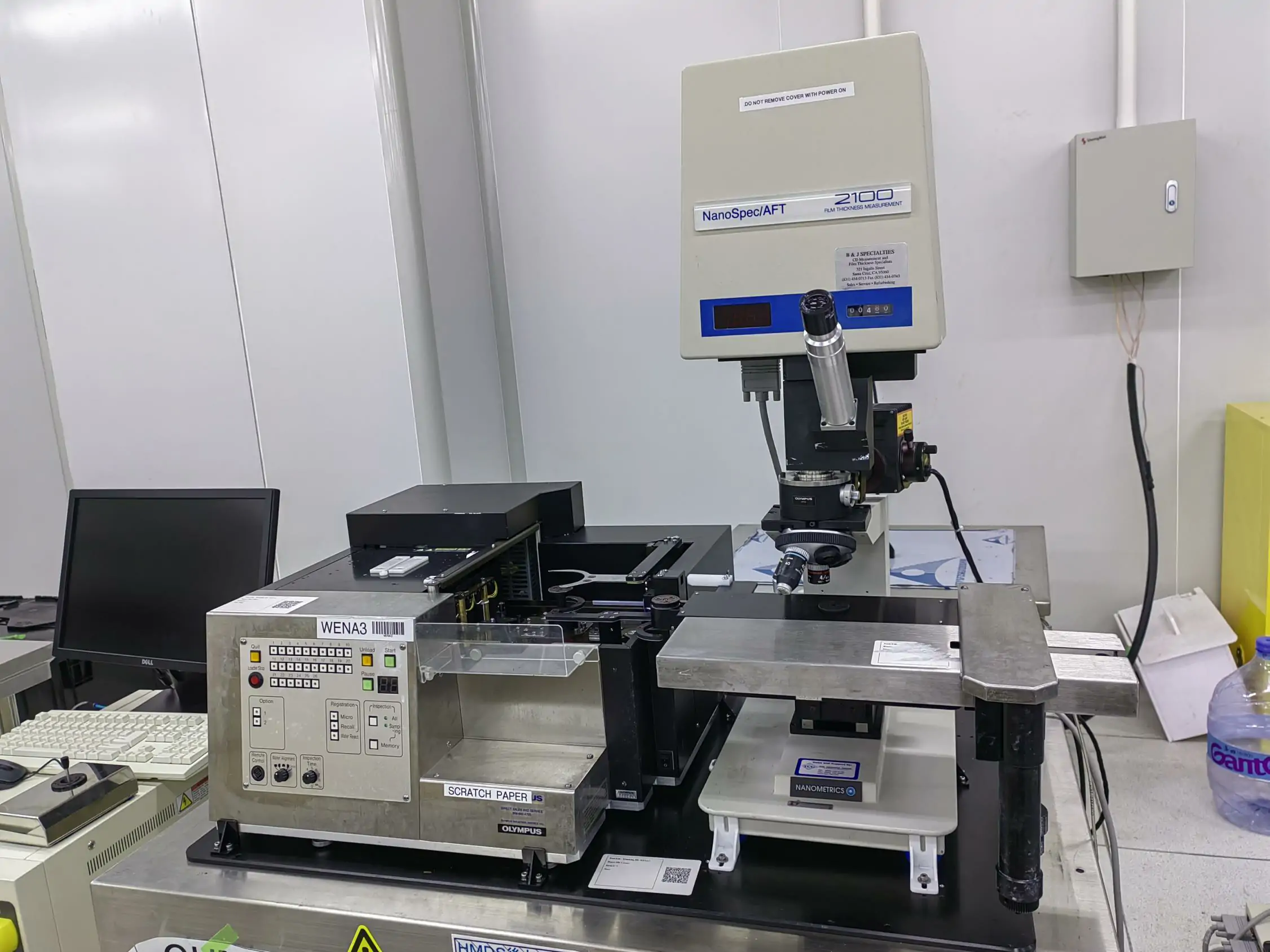
The Nanometrics NanoSpec AFT 2100 is a reliable non-contact film thickness metrology system for semiconductor wafer inspection. Using spectro-reflectometry, it measures transparent thin layers such as oxide, nitride and photoresist, delivering fast readings for routine process monitoring.
Equipped with adjustable microscope objectives and flexible measurement spot size, it provides accurate thickness data without wafer damage. The system verifies film uniformity across substrates and generates repeatable measurement reports, ideal for cleanroom daily quality control.
Compact and robust, this system requires minimal training for operators and keeps maintenance overhead low. It integrates seamlessly into existing cleanroom workflows to maintain tight thin-film control and protect your product yield.

Nanometrics AFT 2100 Main Specifications
| Manufacturer | Nanometrics |
|---|---|
| Product Family | NanoSpec |
| Model | AFT 2100 |
| Equipment Type | Optical Thin-Film Thickness Measurement System |
| Listed Wafer Size | 150 mm / 6-inch |
| Measurement Method | Non-contact spectral reflectance and optical interference |
| Published Wavelength Range | 360–760 nm |
| Published Thickness Range | Less than 100 Å to approximately 50,000 Å |
| Published Reproducibility | Approximately ±2% to ±5%, depending on film and measurement conditions |
| Objective Lenses | 5×, 10× and 50× |
| Published Measurement Spot Sizes | Approximately 50 µm, 25 µm and 5 µm, depending on objective lens |
| Film Requirement | Film should be transparent within the measurement range and have known optical properties |
| Condition | Used semiconductor equipment |
| Availability | Subject to current stock, inspection and configuration confirmation |
