There's a selection question in IC packaging that almost nobody can avoid: flip chip or wire bond? This isn't a question of which technology is more advanced — it's a question of which one fits your product. Flip chip goes further in density and performance, but wire bond still holds a large share of the market on cost and flexibility. Understanding the real gap between the two matters more than chasing the newer technology.
The Connection Method Is Different at the Root
Wire bonding is straightforward: the die faces up, and a very fine gold wire (typically around 25μm in diameter) connects each pad on the die to the substrate or lead frame, one at a time, forming an arc before being cut. A Wire Bonder works like a high-speed sewing machine, completing one bond after another. This approach has been in use since the earliest days of IC packaging, and its core advantages are simplicity, maturity, and low cost.
Flip chip works the opposite way: the die faces down, "flipped" over, with solder bumps built on its pads that press directly onto corresponding pads on the substrate. A Flip Chip Bonder handles this differently from a wire bonder — instead of connecting wires one by one, it aligns the entire bump array and forms all interconnections in a single reflow or thermocompression step. Bump pitch can go below 50μm, and bump counts can reach tens of thousands.
This fundamental difference drives every performance gap that follows.
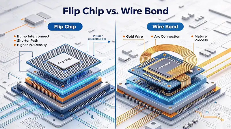
Core Differences Between the Two Technologies
| Comparison Factor | Wire Bond | Flip Chip |
|---|---|---|
| Connection method | Gold wire connects die edge pads to substrate one by one | Solder bumps form area array directly between die and substrate |
| Primary equipment | Wire Bonder | Flip Chip Bonder |
| Electrical path | Passes through gold wire, higher parasitic inductance and capacitance | Extremely short path, significantly lower parasitics |
| Signal integrity | Noticeable attenuation at high frequency, impedance matching difficult | Suited to high frequency and high speed, good signal integrity |
| I/O layout | Die edge only, limited by perimeter | Covers entire die surface, area array layout |
| I/O density | A few thousand approaches the ceiling | Can reach tens of thousands |
| Package thickness | Must accommodate wire arc height, relatively thick | Die-to-substrate face contact, can be made thinner |
| Thermal path | Die backside faces up, higher thermal resistance | Die frontside faces down through bumps, lower thermal resistance |
| Equipment barrier | Low, mature process | High, requires bump fabrication and underfill |
| Changeover flexibility | High, program change is enough | Low, design change requires new bumps or substrate |
| Unit cost | Low, suited to cost-sensitive products | High, more process steps and tighter substrate precision |
| Typical applications | Power management, MCU, memory, LED, consumer chips | High-performance computing, RF front-end, optical modules, advanced sensors |
Electrical Performance: Where Flip Chip Wins, and by How Much
A wire-bonded signal has to travel through a length of gold wire. The wire is short, but the length is still there, and parasitic inductance and capacitance are unavoidable. For high-frequency applications and high-speed signals, that wire run introduces attenuation and impedance mismatch.
Flip chip's connection path is extremely short — bumps connect the die directly to the substrate, cutting signal travel distance from millimeters to micrometers. Parasitics drop substantially, and signal integrity improves noticeably. For RF chips, high-speed logic, and optical communication applications, this gap is decisive. A Flip Chip Bonder's alignment capability directly determines how much of this theoretical advantage makes it into the final product.
Wire bond has no answer here, but the tradeoff is this: if your product doesn't demand high signal integrity, that advantage doesn't buy you anything.
I/O Density and Size: One Hits a Physical Limit, the Other Keeps Going
Wire bond pads must sit along the die edge. A larger die means a longer perimeter, which means more pads. But perimeter grows linearly while die area grows with the square. Once I/O counts climb past a few thousand, edge space runs out completely — a limit that no Wire Bonder improvement can overcome.
Flip chip bumps can cover the entire die surface in an area array. For the same die area, flip chip can provide several times — even ten times — the I/O count of wire bond. That's why high-density logic chips, large-array sensors, and silicon photonics devices almost universally go flip chip.
Flip chip is also more compact. Wire bond needs vertical clearance for the wire arc, making it hard to reduce package thickness. Flip chip is face-to-face contact, so thickness can be pushed down further — important for mobile devices and wearables.
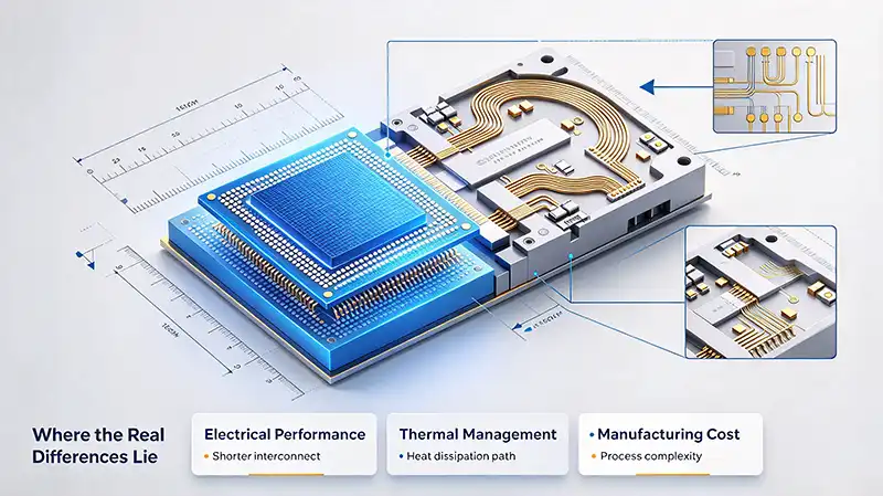
Thermal Management: Flip Chip's Structure Has a Natural Advantage
In wire bond, the die backside faces up, and heat mainly conducts through the silicon to the substrate, resulting in relatively high thermal resistance. In flip chip, the die frontside (where the transistors are) faces down and contacts the substrate directly through bumps and underfill, creating a shorter thermal path over a larger area. For high power density devices, flip chip's thermal performance is clearly better.
Cost and Flexibility: Wire Bond Still Owns the Volume
If performance were the only consideration, flip chip would win almost across the board. But selection isn't only about performance.
Wire bond has lower equipment cost, a mature process, and fast changeover. A Wire Bonder can switch to a new pad layout with nothing more than a program update — no need to redo bumps or redesign the substrate. For mid-to-low volume, high-mix, cost-sensitive products, wire bond's overall cost-performance remains hard to replace.
Flip chip's cost lies in bump fabrication, substrate precision, underfill process, and inspection. The die needs UBM (under bump metallization) and bumps, the substrate needs high-precision pads to match, and after reflow, underfill is required to relieve stress from thermal expansion mismatch. A Flip Chip Bonder must also hold tighter placement accuracy than a wire bonder, which raises both the equipment cost and the process window requirements.
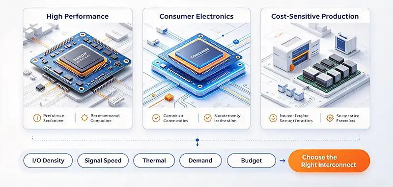
That's why the real-world split looks like this: high-performance computing, advanced sensors, optical modules, and RF front-end go flip chip; power management, MCU, memory, LED, and a large share of consumer chips stay with wire bond.
The Questions That Actually Matter in Selection
What's your I/O count? Past one or two thousand, wire bond's edge layout starts to struggle. Beyond a few thousand, flip chip is essentially the only option.
How high is your signal frequency? High-frequency and high-speed interfaces are sensitive to parasitics, and flip chip's short path shows up directly in performance.
How strict are your thermal requirements? For high power density devices, flip chip's thermal advantage translates into a reliability advantage.
What's your volume, and where's your cost window? In low-volume, high-mix scenarios, a Wire Bonder's changeover flexibility and lower equipment barrier carry more value.
How precise can your substrate be? Flip chip demands tighter line widths, alignment accuracy, and thermal expansion matching. If substrate capability can't keep up, a Flip Chip Bonder's advantages won't materialize.
There are no standard answers to these questions — every product weighs them differently. But laying them out one by one makes the direction clear.
Frequently Asked Questions (FAQ)
Can flip chip completely replace wire bond?
No, and it won't in the foreseeable future. The two serve different application scenarios and cost ranges. Flip chip has clear advantages in high density, high performance, and high thermal demand, but wire bond remains irreplaceable in cost-sensitive, mid-to-low volume, and design-change-heavy scenarios. Many products use both technologies side by side.
What's the minimum bump pitch flip chip can achieve?
Common production bump pitch ranges from 50μm to 200μm. Micro-bumps in advanced packaging can reach 10μm to 30μm, with bump heights of 3μm to 25μm. Tighter pitch places higher demands on Flip Chip Bonder placement accuracy, substrate flatness, and underfill process.
Why does flip chip need underfill?
The die and substrate have different coefficients of thermal expansion. As temperature changes, stress concentrates on the bump joints. Underfill fills the gap between die and substrate; once cured, it distributes stress across the entire adhesive layer, significantly improving connection reliability. Without underfill, flip chip packages are prone to bump cracking in thermal cycling tests.
What matters most when buying a used flip chip bonder?
Alignment accuracy and repeatability come first. Flip Chip Bonder accuracy requirements typically range from ±3μm to ±10μm, and high-precision applications may demand ±1μm or better. During inspection, run standard calibration coupons through multiple cycles and look at repeatability variation, not a single accuracy figure. Then confirm the temperature uniformity of the bump reflow or thermocompression module, the condition of the underfill system, and whether software licenses transfer with the machine. Used Flip Chip Bonder Machines on the market vary widely in condition, and refurbishment quality directly determines the actual accuracy and stability you'll get — always ask the seller for recent measured data.
Does wire bond technology still have room to grow?
Yes, but in different directions. Wire Bonder technology continues to improve in finer wire diameters, lower loop heights, copper wire replacing gold, and bonding speed. For mature-node chips and cost-sensitive applications, these improvements deliver more practical value than switching to flip chip.
The relationship between flip chip and wire bond isn't replacement — it's division of labor. Understanding the logic of that division — when a Flip Chip Bonder's advantages justify the extra cost, and when a Wire Bonder's maturity and flexibility carry more value — is the core skill in packaging selection.