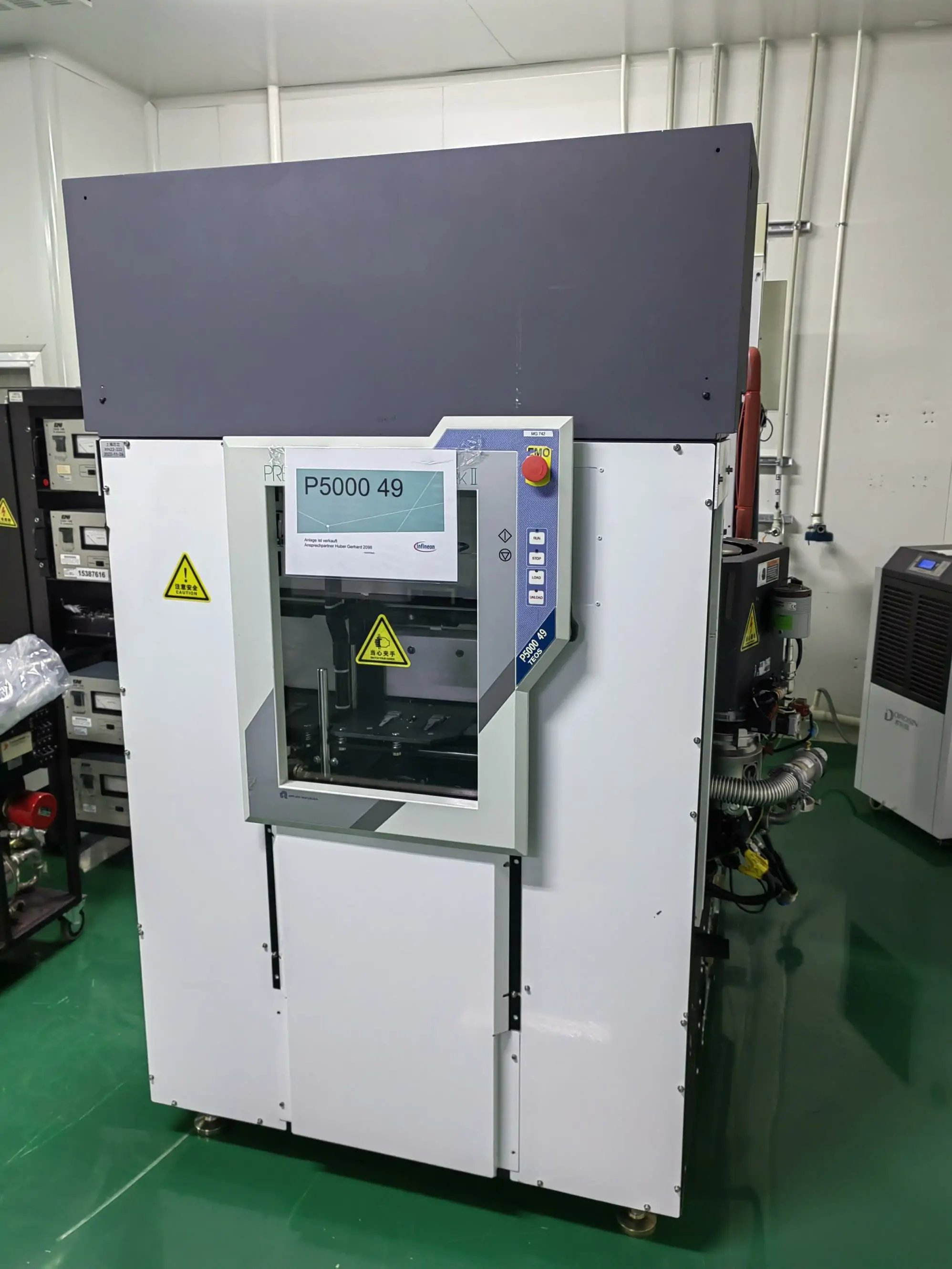
A legendary multi-chamber cluster tool, the Applied Materials P5000 delivers reliable PECVD dielectric deposition for 150mm and 200mm wafer production. It creates silicon nitride, TEOS oxide and oxy-nitride films at low processing temperatures, widely used for passivation and inter-layer dielectric layers.
Its vacuum load-lock architecture protects wafers from ambient contamination. Independent process chambers enable parallel operation, with stable RF plasma control to maintain consistent film thickness and uniformity across batches. Different chamber configurations can be customized to match varied deposition recipes.
This well-established platform enjoys abundant spare parts support globally. Its modular build lowers repair downtime and makes it a practical option for mature-node fabs needing dependable thin-film deposition capacity.

Applied Materials P5000 PECVD Main Specifications
| Manufacturer | Applied Materials |
|---|---|
| Platform | Precision 5000 |
| Model | P5000 PECVD |
| Equipment Type | Single-Wafer Multi-Chamber PECVD System |
| Listed Wafer Sizes | 150 mm and 200 mm wafers |
| Published Platform Capacity | Up to four separate process chambers, depending on configuration |
| Listed Film Materials | SiO2 and SiN |
| Additional Published PECVD Material | Amorphous silicon on appropriately configured systems |
| Published Operating Temperature | Approximately 200–400°C for a representative PECVD configuration; chamber-specific range must be confirmed |
| Wafer Processing | Single-wafer sequential processing |
| Source Listing Status | Listed for sale; current quantity and configuration should be reconfirmed |
| Condition | Used semiconductor equipment |
| Availability | Subject to current stock, chamber configuration and inspection confirmation |

