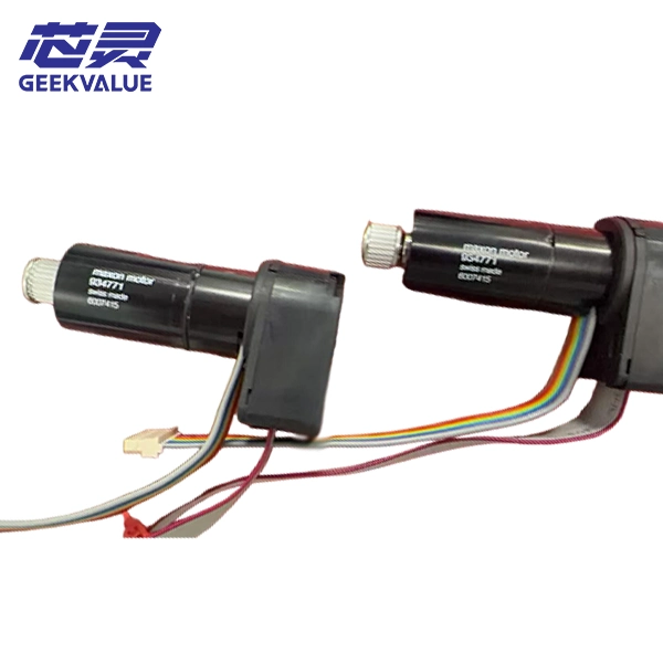
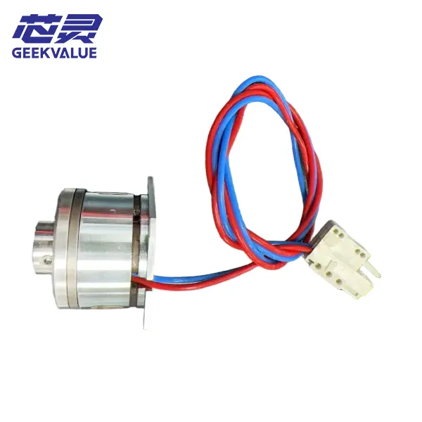
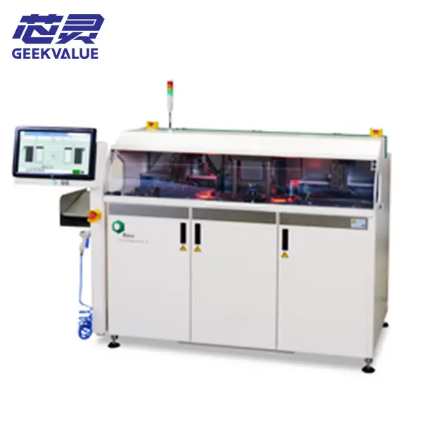
The Besi Datacon 2200 APM high-precision multi-die attach platform enables hybrid die placement within a single machine, mitigating yield and alignment issues in SiP, MCM and hybrid optical power module manufacturing. These defects typically arise when substrates transfer between separate stations. Unlike conventional die bonders limited to a single die type or process, this modular platform delivers seamless transition from R&D prototyping and low-volume trials to mid-volume production. It accommodates 12-inch wafers, waffle packs, Gel-Pak trays and tape feeders without extensive fixture rework. Supported substrates include ceramic carriers, PCBs, lead frames, custom carriers and wafer substrates, allowing packaging houses to reduce recipe setup time between different jobs.
The integrated dispensing unit supports epoxy patterning, stamping and flux dipping, handling materials of varying viscosities within one production run. It covers epoxy bonding, soft soldering, thermocompression and eutectic processes for both hot and cold applications. Face-up and flip-chip placement can run together to meet multi-material assembly requirements for complex heterogeneous packages.
An automatic tool magazine swaps nozzles and ejectors on the fly with no manual downtime. It sequentially attaches dice of different sizes and thicknesses onto the same substrate following programmed coordinates. The vision system delivers fiducial alignment and bad-die skip, paired with thermal compensation to reduce long-run thermal drift and maintain consistent placement accuracy.
Built on an open modular framework, the platform accepts optional upgrades such as extra bond heads, heated bond tools, 3D metrology and UV curing modules. Validated in mass production environments, it maintains reliable uptime for RF modules, sensors, power hybrids and optical SiP assemblies, reducing capital expenditure for factories running multiple packaging projects in parallel.
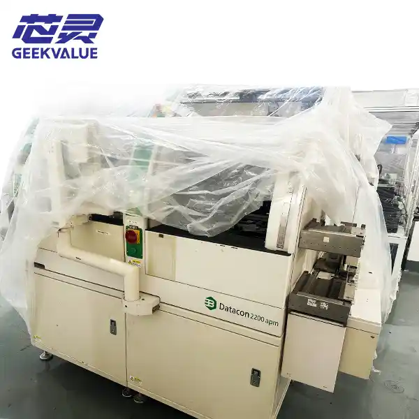
Besi Datacon 2200 APM Multi-Chip Die Bonder Specifications
| Specifications | Details |
|---|---|
| Machine Type | Multi-Chip Heterogeneous Die Attach Platform |
| Primary Application | SiP, MCM & hybrid modules; sequential mixed die placement on a single substrate |
| Placement Mode | Face-up, flip-chip; mixed-run capability |
| Die Feeding Options | 12” wafers, waffle packs, Gel-Pak trays, strip feeders |
| Substrate Carriers | Ceramic carriers, PCBs, lead frames, custom carriers, wafer substrates |
| Integrated Process Station | Built-in dispensing: epoxy patterning, stamping, flux dipping; compatible with multi-viscosity materials |
| Bonding Processes | Epoxy attach, soft soldering, thermocompression, eutectic bonding; hot & cold processes |
| Tool Changer | Automatic tool magazine, on-the-fly nozzle / ejector swap, no manual interruption |
| Vision & Compensation | Fiducial alignment, bad die skip; thermal compensation to minimize long-run thermal drift |
| Optional Upgrades | Additional bond heads, heated bond tools, 3D metrology, UV curing module |
| Production Profile | R&D validation, low & medium volume runs; optimized for frequent product changeovers |
| Target Packages | RF modules, sensor packages, power hybrids, optical SiP assemblies |
| Platform Design | Open modular architecture, customizable configuration to cut capital cost for multi-project operation |
Notes: The above table outlines base specifications for the Besi Datacon 2200 APM Multi-Chip Die Bonder. Actual performance, accuracy and process capability depend on selected options, die geometry, adhesive material, substrate design and factory ambient conditions. UPH and placement yield need to be verified under real process recipes. Custom process evaluation and configuration consultation are available upon request.