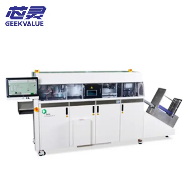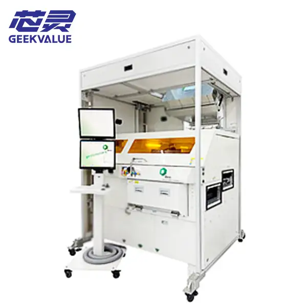
The BESI Datacon 8800 CHAMEO ultra plus AC is a benchmark C2W (Chip-to-Wafer) hybrid bonding system for advanced packaging, an ideal platform for Chiplet, 3D IC heterogeneous integration and Cu-Cu hybrid bonding processes.
Equipped with the Van Gogh high-precision optical alignment system, it delivers nanometer-level placement accuracy of 100 nm @ 3σ, perfectly meeting the stringent alignment requirements of fine-pitch interconnection. Its ISO 3 clean working chamber effectively controls particle contamination to secure high yield for thin wafers and ultra-thin die pick-and-place. Featuring dual bonding heads, it achieves a dry cycle throughput up to 2000 CPH. Integrated with in-line IR inspection, automatic nozzle change and EFEM automated wafer handling interface, the system offers robust process stability for both R&D prototyping and low-volume mass production.
This used unit has undergone comprehensive maintenance, motion axis calibration, optical alignment validation and full inspection of vacuum systems, with all core performance parameters verified. Compared with brand-new equipment, it significantly cuts capital expenditure, enabling enterprises to quickly set up hybrid bonding pilot lines and seize the R&D window for advanced packaging. Suitable for high-end packaging projects such as computing chips and memory stacking.

CHAMEO ultra plus AC Specifications
| Specification | Published Value |
|---|---|
| Process | Hybrid bonding |
| System Accuracy | 100 nm @ 3σ alignment worst corner GOG |
| Accuracy Self Check | Single BMC kit |
| Cleanliness | ISO 3 in working area |
| Throughput | Up to 2,000 CPH, dry cycle |
| Substrate Wafer | 12-inch wafer through EFEM |
| Substrate Wafer Thickness | 0.5 to 2.0 mm |
| Component Supply | 12-inch film frame or 12-inch wafer carrier, silicon or glass carrier |
| Die Size | 0.5 × 0.5 mm to 33 × 28 mm |
| Die Thickness | 25 μm to 800 μm |
| Die Ejection | Needle, Multi Stage, UV on request |
These are platform specifications. EFEM setup, inspection hardware, tool changing, die-ejection method, automation interface, and other installed options still need to be confirmed on the actual machine.