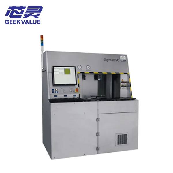
ThinkLaser SigmaDSC performs automated hard marking on semiconductor wafers. Its core assembly combines Dual-Spot Optics™, diode-pumped solid-state laser source and closed-loop depth control to form permanent dot-matrix indent marks. Marks retain readability across successive thermal cycling, etching and polishing steps.
The integrated optical engine supports calibrated spot adjustment via software between 50 μm and 110 μm. Geometry changes require no hardware swap during production runs. Pulsed laser output maintains minimal pulse variation, sustaining consistent dot circularity and aspect ratio across batches. Indent depth settings are programmable. Closed-loop sensors capture live laser metrics and feed data into SPC logging streams. Mark dimensional consistency can be tracked without repeated manual sampling.
Automated Substrate Handling & Cleanroom Alignment Performance
Wafer transport mechanics load and unload 100 mm to 300 mm substrates inside cleanroom environments. Marking coordinates align to SEMI layout conventions. Dot-matrix hard ablation generates deep, high-contrast identifiers. Vision systems and OCR read these marks through every manufacturing stage. Tunable process controls balance indent depth, line speed and particulate output for continuous silicon wafer traceability operations.

Process & Operational Benchmarks
Table: Core process specifications of ThinkLaser SigmaDSC wafer hard marking system
| Parameter | Specification |
|---|---|
| Supported wafer size | 100 mm / 200 mm / 300 mm |
| Laser mark spot range | 50 μm – 110 μm |
| Marking pattern | Dot-matrix indent hard mark |
| Depth control | Real-time closed-loop sensing |
| Standard compliance | SEMI mark layout compatible |
| Data logging | SPC compliant traceability records |
This benchmark table captures core process metrics; full detailed parameters are available via product datasheet download.