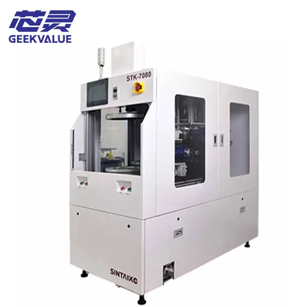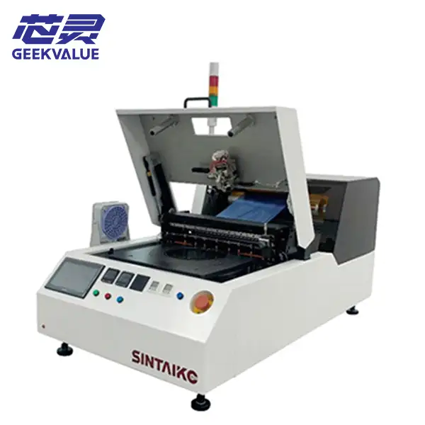
The SINTAIKE STK-6020 wafer mounter performs tape lamination for semiconductor wafers before back grinding. Its roller-based lamination framework controls tension, thermal distribution and electrostatic state throughout the tape bonding cycle to achieve consistent adhesion across wafer surfaces. The unit runs semi-automatic sequences: operators load substrates, then the machine handles film unwinding, roller bonding and edge trimming. It works with blue dicing tape and UV release tape for silicon and compound semiconductor wafers in pilot and mid-volume cleanroom workflows.
Analysis of Core Technologies of the SINTAIKE STK-6020 Wafer Laminator
The machine’s core is the contact roller lamination assembly. It maintains continuous and uniform roller pressure across the wafer plane, reducing trapped air that causes delamination and chipping during subsequent thinning. Temperature synchronisation between the roller and anti-static platen stabilises adhesive behaviour, avoiding localised overheating or weak bonding spots.
Multi-stage ESD suppression integrates ionised air, conductive chuck and anti-static roller coatings to neutralise charge build-up. This limits electrostatic damage to sensitive compound substrates. The tape feed spool mechanism delivers constant unwinding tension, preventing tape stretch, wrinkles and uneven bonding on thin wafers.
A dual cutting module combines straight and heated circular blades. Heating at the cutting point softens tape edges, cutting down residual burrs and extra manual trimming work. Pneumatic locating pins align wafers via flat edge or V-notch references, supporting quick transitions between 6-inch and 8-inch wafer formats.
All process parameters sit within a PLC touch HMI. Recipes store tension, speed and temperature profiles, which operators recall or adjust directly. Changeover between tape types and wafer sizes takes minutes, fitting mixed-lot processing. Safety interlocks and emergency stop circuits run through the whole operation cycle.

SINTAIKE STK-6020 Process Performance Benchmark Table
| Process Item | Working Range | Practical Performance |
|---|---|---|
| Supported wafer size | 6 inch / 8 inch | Fast format swap without chuck replacement |
| Applicable wafer thickness | 300 μm – 750 μm | Stable lamination for thin and standard silicon / compound wafers |
| Compatible tape type | Blue dicing tape, UV release tape | Accommodates a wide range of adhesive strength grades |
| Lamination bubble rate | Controlled under low incidence | Reduced rework before wafer backside thinning |
| Alignment tolerance | Precision pin positioning | Maintains consistent offset for V-notch and flat-edge substrates |
| Single cycle time | Semi-auto sequence, lot dependent | Balanced throughput for pilot and medium-volume cleanroom lots |
Application
This tape lamination system applies protective backing tape for wafer back thinning. Compatible substrates include silicon, GaAs and other compound wafers. It fits cleanroom stations for low and medium batch manufacturing, process validation lines and OSAT sites.