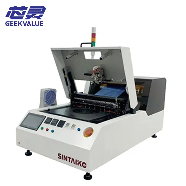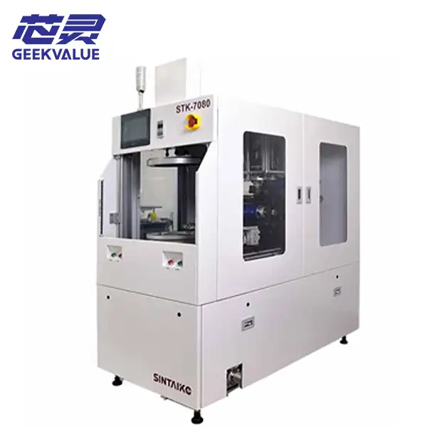
The STK-7080 is a semi-automatic wafer vacuum mounter developed for compound semiconductor, MEMS and thin wafer temporary bonding applications. It accommodates 4–8 inch wafers with thickness of 100–750 μm and supports Si, SiC, GaAs and GaN substrates.
It adopts non-contact vacuum mounting, avoiding mechanical stress caused by conventional roller lamination and significantly reducing breakage risk for thin wafers and high-cost wide-bandgap substrates. It delivers ±0.5 mm mounting accuracy, throughput ≥60 wafers/hour and ≥99.9% yield with bubble-free lamination (particle contamination excluded). Equipped with a ULVAC vacuum pump, PLC and 10-inch touchscreen for recipe storage. MTBF>500 h, MTTR<1 h and planned downtime ≤3% to secure high uptime. Standard configurations include light curtain, E-stop and deionizing fan for ESD control.
This pre-owned unit comes with auto film feeding, cutting and waste collection. It can start production without modification. Featuring mature design and high spare part commonality for easy maintenance, it is well suited for flexible small-to-medium batch production and helps reduce project CAPEX.

SINTAIKE STK-7080 Technical Specifications
| Parameter | Description |
|---|---|
| Equipment Type | Non-contact vacuum wafer mounter |
| Manufacturer | SINTAIKE |
| Technology | Roller-free vacuum lamination |
| Wafer Size | 4 inch - 8 inch wafer |
| Wafer Material | Silicon, SiC, GaAs, GaN |
| Wafer Thickness | 100μm - 750μm |
| Film Type | Blue film / UV film |
| Position Accuracy | Approximately ±0.5mm |
| Control System | PLC control with touchscreen interface |
| Operation Mode | Semi-automatic |
Specifications may vary depending on equipment configuration and customer process requirements.