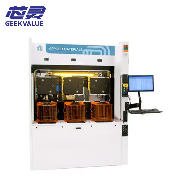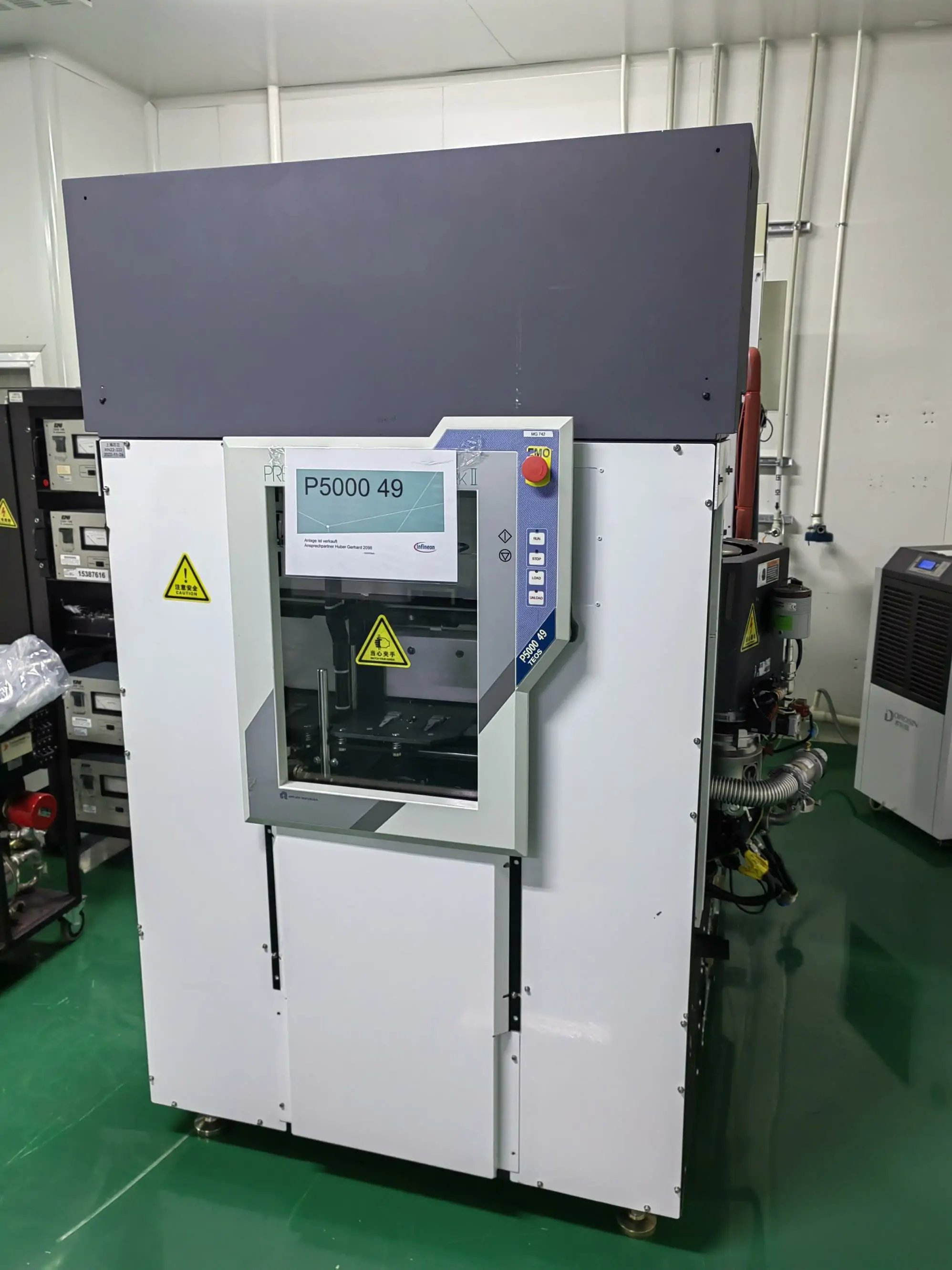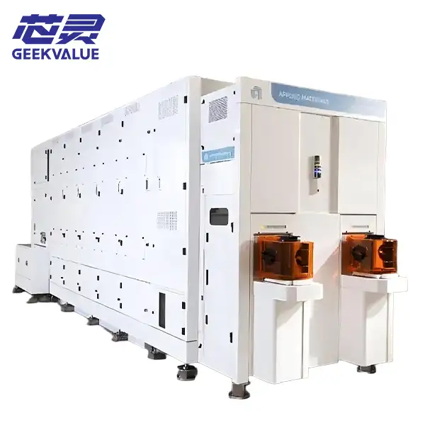
For advanced packaging metallization, the Applied Materials Nokota ECD System offers a trusted electrochemical deposition platform. It specializes in copper plating for wafer-level RDL and micro bump formation, critical building blocks for modern heterogeneous chip integration.
Controlled electrolyte flow and real-time current regulation maintain even copper coverage across the wafer. This reduces thickness variance and helps cut down on plating-related defects. Flexible recipe setup accommodates diverse bump designs and wafer formats, fitting smoothly into high-volume packaging lines to support consistent device performance.