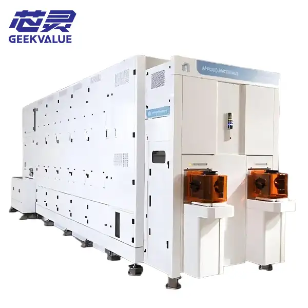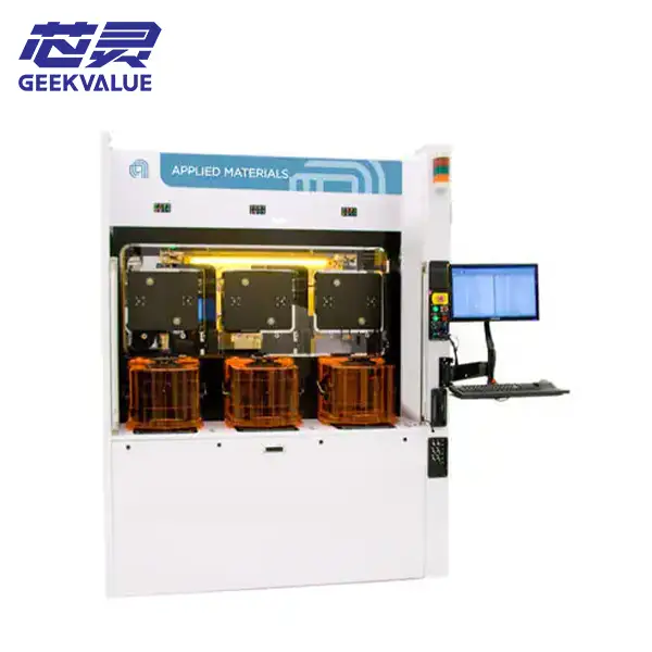
Applied Materials' Raider® Edge ECD single-wafer plating platform supports 150mm, 200mm, and 300mm wafer sizes; its configurable architecture offers manufacturers the flexibility to accommodate diverse wafer sizes, substrate types, and production requirements. Applied Materials describes the Raider Edge ECD as a platform capable of supporting a wide range of applications, including metal and alloy plating, etching, cleaning, and dielectric layer processes.
Combining a compact system footprint with high-throughput wafer handling and multi-chamber processing capabilities, the platform is ideally suited for semiconductor fabs, advanced packaging facilities, research centers, and production lines requiring controlled electrochemical deposition processes.
Applied Materials Raider® Edge ECD – Technical Specifications
| Specification | Details |
|---|---|
| Manufacturer | Applied Materials |
| Model | Raider® Edge ECD |
| Equipment Type | Single-Wafer Electroplating Platform |
| Process Technology | Electrochemical Deposition (ECD) |
| Process Application | Metal Deposition |
| Wafer Processing | Single-Wafer Processing |
| Key Application Areas | Semiconductor Interconnects and Advanced Packaging |
| Equipment Condition | Used Equipment |
| System Configuration | Subject to Available Equipment Configuration |