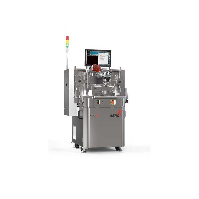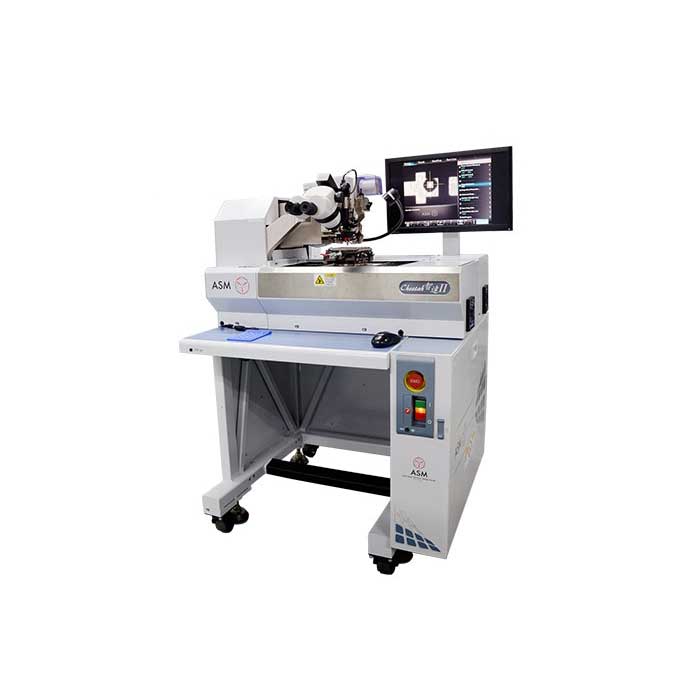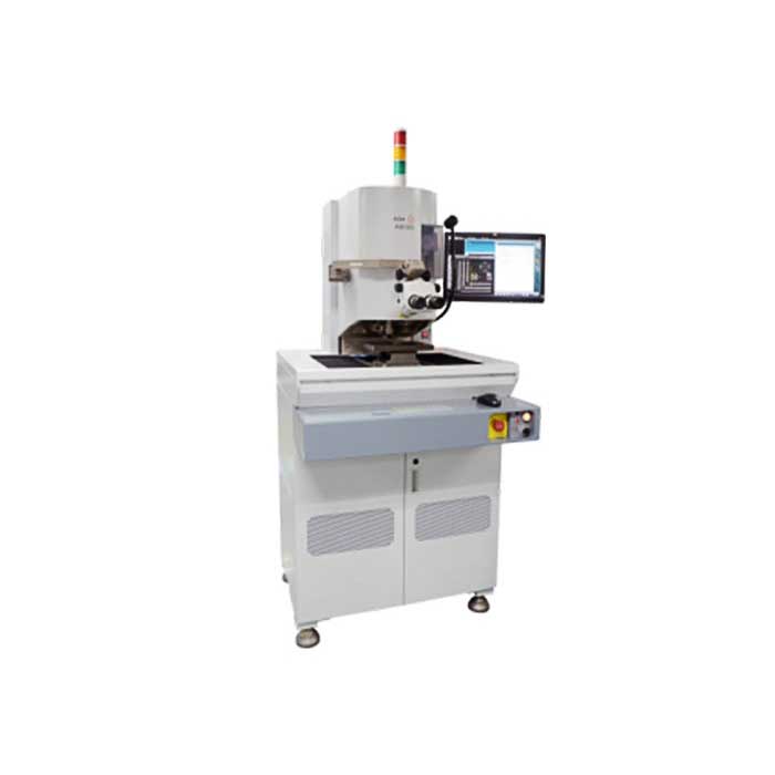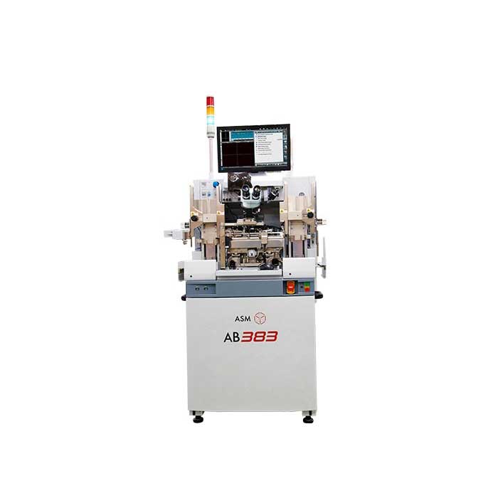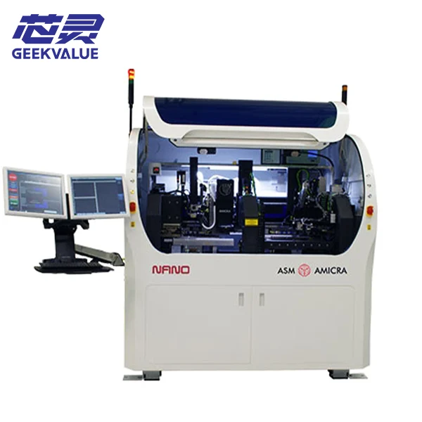
Sub-micron alignment determines the performance of photonic and high-density chip assemblies. The ASMPT AMICRA NANO delivers ultra-precise flip chip bonding with placement accuracy down to ±0.2µm @ 3σ.
Built on a vibration-isolated granite base, it integrates high-resolution optical alignment and dynamic offset correction. Multiple bonding modes are supported, including eutectic bonding, laser soldering, epoxy dispensing and in-situ UV curing. Its internal HEPA cleanroom and ionizer maintain stable conditions for delicate optical and silicon photonic components.
Modular configuration supports 300mm substrate processing and post-bond inspection. It maintains consistent alignment repeatability to reduce assembly defects for CPO, silicon photonics and direct bond interconnect projects.

Technical Specifications (Typical Configuration)
Performance values vary depending on process module, die geometry, and substrate configuration.
| Parameter | Typical Description |
|---|---|
| System Type | Ultra-precision flip chip and die bonding platform |
| Placement Accuracy | ±0.5 μm to ±2 μm @ 3σ (process and configuration dependent) |
| Supported Processes | Thermocompression bonding / Mass reflow / Eutectic bonding |
| Wafer Size Support | Up to 8-inch or 12-inch (system dependent) |
| Substrate Compatibility | Ceramic carriers, silicon interposers, laminated substrates |
| Throughput | Optimized for high-precision, low-to-medium volume manufacturing |