Particles and haze do not affect every part of a wafer in the same way. Their distribution across the surface can reveal differences in substrate cleanliness and film quality, making wafer-level defect mapping an important part of incoming material control.
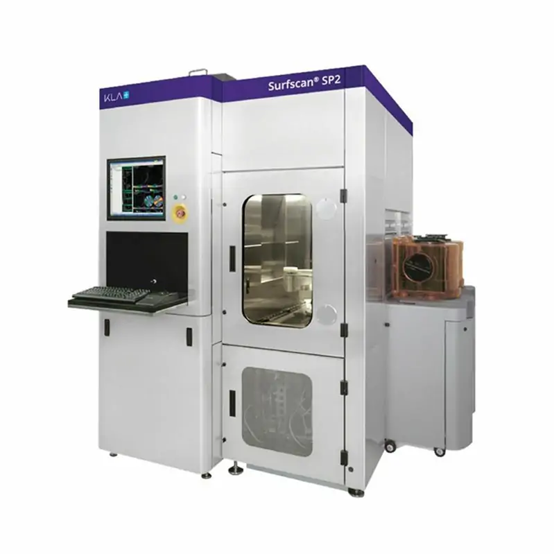
The KLA Surfscan SP2 inspects unpatterned wafers using laser-based optical detection. Its inspection results help identify surface anomalies, including particles and haze, before wafers proceed to lithography, deposition or other fabrication steps. Both bare silicon wafers and certain film-coated substrates may be inspected, depending on the measurement recipe and system configuration.
For wafer manufacturers, the key output is not simply a pass-or-fail result, but a clearer picture of surface conditions across the wafer.
KLA Surfscan SP2 Main Specifications
| Manufacturer | KLA-Tencor / KLA |
|---|---|
| Model | Surfscan SP2 |
| Equipment Type | Unpatterned Wafer Defect Inspection System |
| Supported Wafer Sizes | 200 mm and 300 mm |
| Inspection Technology | UV laser dark-field optical inspection |
| Published Sensitivity | Defects as small as approximately 37 nm under specified wafer and inspection conditions |
| Illumination Modes | Normal-incidence and oblique-incidence illumination |
| Inspectable Surfaces | Bare wafers, smooth and rough films, film stacks and photoresist layers |
| Data Capability | Defect mapping, classification and SURFimage surface-analysis data |
| Condition | Used semiconductor equipment |
| Availability | Subject to current stock, inspection and configuration confirmation |