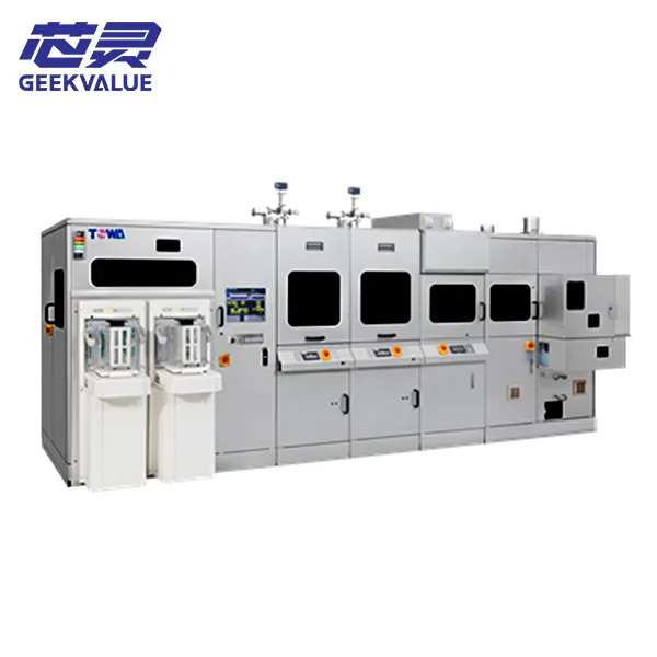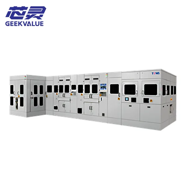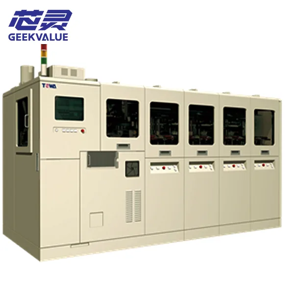
Engineered for mass production of leadframe packages, the TOWA Y1E4120 Transfer Molding System executes robust transfer molding to encapsulate semiconductor dies. The cured epoxy layer shields delicate chip circuitry from humidity, particle pollution and mechanical damage throughout subsequent assembly and application.
Fine-tuned clamping force and resin injection control suppress voids and excess flash. Fast mold change capability reduces downtime, matching the needs of packaging facilities running mixed device types and continuous high-volume manufacturing.

TOWA Y1E4120 Machine Information
| Manufacturer | TOWA |
|---|---|
| Model | Y1E4120 |
| Equipment Type | Modular semiconductor transfer molding system |
| Workpiece Type | Substrate and leadframe |
| Workpiece Length | 100–260 mm according to the manufacturer’s model specification |
| Workpiece Width | 15–78 mm according to the manufacturer’s model specification |
| Molding Compound Diameter | Ø13, 14, 16, 18 or 20 mm |
| Molding Compound Length | 11.7–35.0 mm |
| Clamp Capacity | 392–1,176 kN / 40–120 tf, depending on configuration |
| Press Configuration | One to four press modules according to the model configuration |
| Standard Machine Time | Approximately 20 seconds; actual cycle time depends on the product, mold and process |
| Condition | Pre-owned semiconductor packaging equipment |
| Actual Configuration | Confirmed according to the specific machine available |
| Delivery Scope | Based on the quotation and confirmed equipment list |
| Shipping | Export packing and worldwide delivery |