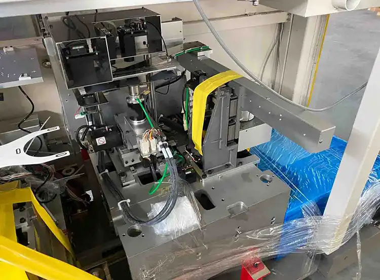
The Canon Anelva FC7100 is a robust PVD sputtering system built for metal and dielectric film deposition on semiconductor wafers. This cluster platform handles titanium, titanium nitride, aluminum and other conductive layers, serving metallization steps for discrete and power device manufacturing.
Equipped with multiple sputtering targets and high-precision wafer staging, it achieves excellent film uniformity and step coverage. The integrated load-lock chamber preserves vacuum integrity, reducing particle contamination during wafer transfer and boosting process repeatability.
Simple chamber maintenance and easily sourced consumables keep running expenses under control. It fits smoothly into 150/200mm fab workflows to deliver consistent metal deposition and support stable device yield.

Canon Anelva FC7100 Main Specifications
| Manufacturer | Canon Anelva |
|---|---|
| Model | FC7100 |
| Equipment Type | Cluster-Type PVD Sputtering System |
| Supported Wafer Size | 300 mm / 12-inch wafers |
| Primary Process | Physical vapor deposition and reactive sputtering |
| Primary Published Application | High-k metal-gate film formation |
| Maximum Installed Modules | Up to five modules in the published platform |
| Configurable Module Types | Sputtering, etching, oxidation and heating, depending on configuration |
| System Architecture | Cluster platform |
| Listed Service Year | 2011, according to the available equipment page |
| Condition | Used semiconductor equipment |
| Availability | Subject to current stock, module configuration and inspection confirmation |