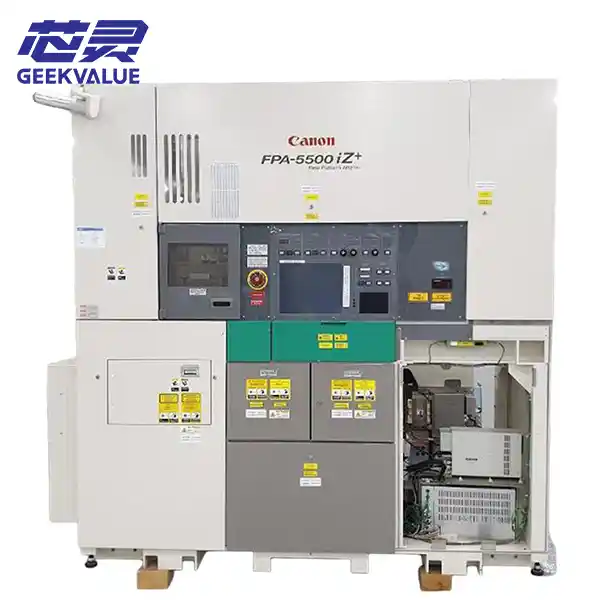
The Canon FPA-5500iZ+ brings 365 nm i-line lithography to semiconductor manufacturing processes that require consistent pattern transfer across wafer surfaces. Its 4:1 reduction optics project mask patterns onto the wafer, with a maximum exposure field of 26 × 33 mm. The platform supports both 200 mm and 300 mm wafer processing, depending on the installed configuration.
Image placement depends on more than optical resolution alone. Alignment performance, exposure distortion correction and adjustable numerical aperture all influence pattern fidelity from field to field. The system’s mask protection features help reduce the risk of reticle damage and particle-related defects, while wafer handling affects throughput and photoresist condition during repeated exposure cycles.
Applications may include power semiconductor devices, CMOS image sensors and MEMS, where i-line lithography remains relevant to established manufacturing flows. For production lines evaluating a used FPA-5500iZ+, wafer-size configuration, overlay performance, optical condition and service history are important points to verify before purchase.