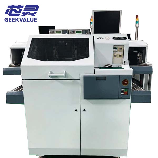
The ASMPT ALSI LASER1205 enables precision multi-beam laser dicing and grooving. Its proprietary multi-beam laser optics and wafer-stepping motion control technology minimize thermal damage while ensuring high throughput.
By processing with multiple laser beams simultaneously, energy is evenly distributed along the dicing path, thereby reducing localized heat accumulation; this approach effectively protects fragile low-k dielectric layers and thin dies, preventing cracks or structural integrity issues. The system performs real-time monitoring of the dicing kerf during processing to detect defects early and minimize scrap. It is suitable for both bare wafers and wafers mounted on dicing tape frames, and supports a wide range of substrate thicknesses.
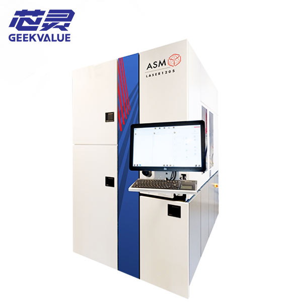
Key Features:
Multi-Beam Technology: Patented multi-beam laser process achieves a cutting width of less than 12μm on 100μm silicon wafers. Low power per beam but many beams enable high material removal rates with minimal heat-affected zone (HAZ < 2μm).
Ultra-Thin Wafer Capability: Processes wafers ranging from 10μm to 250μm in thickness with positioning accuracy and reproducibility of less than 1.5μm — operating approximately 50% faster than conventional laser dicing methods.
Patented V-Process for Full-Cut Dicing: Enables full-cut dicing of Low-K (thin) Si wafers including DAF or FOW while achieving high die strength (450-500MPa) and low burr (<5μm). A single process step eliminates extra production steps required by DBG or hybrid dicing technologies.
Precision Slider Concept: The unique wafer stepper concept allows high accuracy and reproducibility across all processing conditions.
Technical Specifications:
| Specification | Unit | Value |
|---|---|---|
| Processing Method | – | Multi-Beam Laser Dicing |
| Wafer Thickness Range | μm | 10 – 250 |
| Positioning Accuracy | μm | < 1.5 |
| Cut Width (100μm Si) | μm | < 12 |
| Heat Affected Zone (HAZ) | μm | < 2 |
| UV Wavelength | nm | 355 |
| IR Wavelength | nm | 1064 |
| Wafer Size | inch | Up to 12 |
Applications:
Ideal for SiC power device singulation, GaAs RF chip dicing, Low-K thin wafer separation, MEMS device cutting, and advanced packaging applications requiring minimal thermal damage.