The ASMPT AD838L-Plus is a fully automatic die bonder developed for large and surface-sensitive substrates. Its distinguishing feature is dragging-free indexing, which reduces uncontrolled contact with the substrate during transport.
ASMPT publishes a maximum substrate size of 300 × 100 mm. A high-precision configuration with ±15 μm @ 3σ XY placement accuracy was also available as an option.
These capabilities depend on the installed transport, workholder, vision system and tooling. A used AD838L-Plus should therefore be matched to the actual substrate drawing and placement requirement before its condition or production value can be determined.
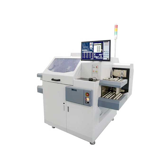
When an AD838L-Plus Is Worth Considering
The AD838L-Plus is most relevant when the receiving material is long, fragile, easily scratched or sensitive to uncontrolled contact during indexing.
Its material-handling design may provide a practical advantage for substrates that cannot be pushed or dragged reliably through a conventional transport system. That advantage depends on the condition and geometry of the installed rails, supports, clamps and workholder.
The model is less suitable when the project requires several-micron placement accuracy or confirmed flip-chip handling but the available machine has only the standard vision and die-placement configuration.
Published AD838L-Plus Specifications
| Manufacturer | ASMPT / ASM Pacific Technology |
|---|---|
| Model | AD838L-Plus |
| Equipment Type | Fully automatic die bonder |
| Material Transport | Dragging-free substrate indexing |
| Maximum Substrate Size | Up to 300 × 100 mm* |
| High-Precision Option | ±15 μm @ 3σ XY placement accuracy* |
| Bond Head | High-throughput bond-head design |
| Material Handling | Automatic material-handling system |
| Automatic Wafer Loader | Optional |
| Flip-Chip Handling | Not identified by ASMPT as a standard AD838L-Plus feature; confirm from the installed machine |
*Published platform values. ASMPT states that performance depends on the package and material. The exact machine configuration and production material determine the achievable result.
Why Dragging-Free Indexing Matters
In a conventional transport system, a long substrate may slide across rails or supporting surfaces as it advances. This can be unsuitable when the underside, coating, metallization or completed units must remain free from contact damage.
The AD838L-Plus uses a dragging-free indexing concept to control substrate movement. The effectiveness of this system depends on more than the maximum published dimensions.
The following substrate information is required:
Overall length, width and thickness
Material stiffness and allowable bending
Flatness and maximum permitted warpage
Permitted edge-clamping area
Surfaces that must remain free from contact
Unit layout and bond-site positions
Indexing direction and indexing pitch
Input and output carrier format
A substrate falling within 300 × 100 mm is not automatically compatible. It may still require different rails, clamps, supports or a product-specific workholder.
Testing the Substrate Transport
The transport system should be tested with material of comparable dimensions, stiffness and surface condition. An empty transport cycle confirms mechanism movement but does not show how the substrate behaves under production conditions.
A complete transport test should cover:
Loading the substrate into the machine
Initial substrate recognition and positioning
Repeated full-length indexing
Clamping and release at each bond position
Support of the substrate near the bonding area
Movement of warped or flexible material
Unloading after the placement sequence
After the test, the substrate should be inspected for scratches, edge marks, bending, unstable clamping and position shift. Transport performance is central to the value of this model and should not be reduced to an axis-movement video.
Verifying the Optional ±15 μm Configuration
The published ±15 μm @ 3σ XY placement accuracy belongs to the optional high-precision configuration. It is not a universal specification for every AD838L-Plus.
The configuration should be identified through the installed optics, option records, software functions and machine documentation. Current performance must then be measured rather than inferred from the original model specification.
An accuracy test should include:
Vision-camera and lighting inspection
Pattern-recognition stability
Bond-head and stage calibration
Encoder and motion-system response
Repeated placement on measurable sample material
XY measurement across multiple substrate positions
A sufficient sample quantity to evaluate placement distribution
A single accurately placed die does not establish a 3σ result. The sample quantity, measurement equipment and acceptance limits should be defined before testing.
For processes requiring approximately ±3 μm placement, the ASMPT AD280 Plus high-precision die bonder is a more appropriate platform to evaluate.
Confirming Flip-Chip Capability
ASMPT’s current AD838L-Plus product information does not list flip-chip handling as a standard feature. The model name alone therefore does not confirm that a particular machine can invert, align and place dies face-down.
Flip-chip capability can only be confirmed when the required physical modules and software are present. The configuration should include:
A die-inversion or face-down presentation mechanism
Upward-looking optics or another suitable alignment arrangement
Software functions for the required die orientation
Compatible pickup and placement tools
Protection for the active or bumped die surface
Suitable substrate recognition and alignment functions
The required adhesive, flux or bonding-process hardware
The process test must show the die being handled in its required orientation. A standard face-up die-placement test does not confirm flip-chip operation.
The later AD838L-G2 is separately identified by ASMPT as having flip-chip handling and up-look pattern recognition. Functions published for the AD838L-G2 should not be assigned automatically to an earlier AD838L-Plus.
AD838L-Plus Compared with Other ASMPT Die Bonders
| Model | Confirmed Platform Strength | Key Distinction |
|---|---|---|
| AD838L-Plus | Dragging-free handling for substrates up to 300 × 100 mm | ±15 μm was optional, and flip-chip capability must be confirmed from the installed configuration |
| AD838L-G2 | High-throughput die bonding with published flip-chip handling and up-look PR | G2 functions should not be assumed to exist on the AD838L-Plus |
| AD8312Plus | 12-inch wafer handling and high-density leadframe epoxy production | More relevant when wafer capacity and conventional epoxy die attach determine the equipment choice |
| AD280 Plus | Published ±3 μm placement accuracy and flip-chip handling | More suitable when placement precision is more important than long-substrate throughput |
The receiving material, die orientation and placement tolerance separate these platforms more clearly than general descriptions such as “automatic,” “high-speed” or “high-precision.”
Inspection Scope for a Used AD838L-Plus
Machine Identity and Configuration
Confirm the complete model designation on the nameplate
Record the serial number and manufacturing year
Identify the previous substrate and production process when records are available
Record the installed software version and enabled options
List the vision, wafer and material-handling modules
Substrate-Handling System
Inspect rails, supports, clamps and workholder surfaces
Check loaders, unloaders and carrier interfaces
Test the full indexing range
Inspect for worn contact surfaces and damaged locating features
Check clamping repeatability at each bond position
Die Pickup and Placement
Inspect the wafer table, expander and ejector system
Check vacuum response and pickup stability
Inspect the bond head and installed collet
Test vision recognition and placement across the substrate
Record pickup failures, placement rejects and recurring alarms
Optional Functions
Measure placement results if the ±15 μm option is included
Test automatic wafer loading if the loader is installed
Run the complete die-inversion sequence if flip chip is required
Test any installed dispensing, stamping or process-specific hardware
The completed inspection record should distinguish power-on testing, substrate-transport testing, die-placement testing and measured accuracy. These are different levels of verification.
Available Machine Configuration
| Model and Serial Number | Confirmed from the current machine nameplate |
|---|---|
| Manufacturing Year | Confirmed from the nameplate or machine records |
| Previous Application | Previous substrate and process information provided when available |
| Substrate Transport | Installed rail range, workholder, clamps, loader, unloader and transport direction |
| Wafer System | Wafer format, frame type, wafer table, expander and ejector configuration |
| Automatic Wafer Loader | Listed only when physically installed and tested |
| Precision Option | Option status and available placement-measurement results |
| Flip-Chip Configuration | Die-inversion, up-look vision, software and tooling listed separately when installed |
| Bonding Process | Installed adhesive or process-specific modules identified from the physical machine |
| Included Tooling | Workholders, rails, clamps, collets, ejector tools, magazines and fixtures |
| Software and Backups | Software version, licenses, configuration files and available product recipes |
| Test Status | As-removed, powered on, transport-tested, placement-tested or process-tested |
Used AD838L-Plus Availability
AD838L-Plus availability should be stated together with the installed substrate-handling, wafer and vision configuration. Precision, wafer automation and possible flip-chip functions may differ between machines carrying the same model name.
Send the substrate drawing, die dimensions, wafer format, die orientation, required placement tolerance and bonding process through our equipment inquiry form. The information will be compared with the physical machine, installed options and included tooling.