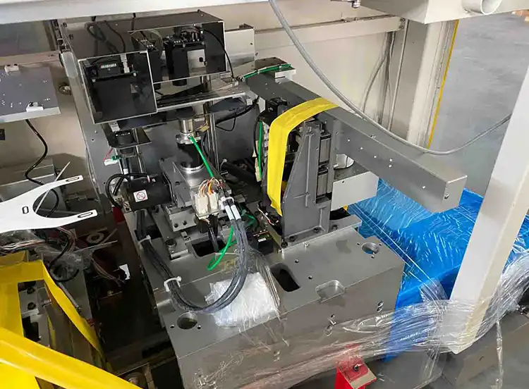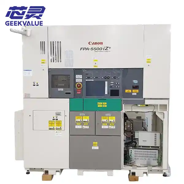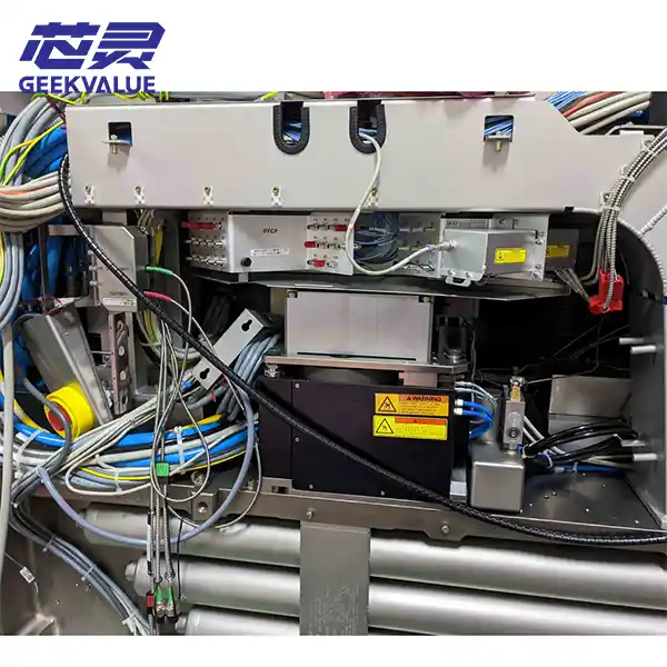
The ASML XT 760F is a high-precision DUV step-and-scan lithography system, built for patterning semiconductor wafers in mature-node manufacturing. Equipped with advanced projection optics and dual-stage wafer platform, it delivers reliable overlay control and stable imaging performance for 200/300 mm silicon substrates.
It integrates automatic focusing, wafer shape correction and flexible illumination modes to maintain consistent critical dimension (CD) uniformity across the whole wafer. The system compensates for wafer warpage and mask distortion, minimizing pattern shift and edge defects during continuous exposure cycles. Its high optical transmission supports stable throughput and wide process window for mass production.
This litho tool is widely deployed for power devices, discrete semiconductors, CMOS image sensors and MEMS chips. It handles non-critical layers in backend advanced packaging, offering low ownership cost and excellent process repeatability for OSAT and mid-node fabs.

Key Technical Parameters
| Item | Specification |
|---|---|
| Lithography Type | DUV Step & Scan |
| Wavelength | 248 nm KrF |
| Supported Wafer Size | 200 mm / 300 mm |
| Minimum Resolution | 0.13 μm |
| Overlay Accuracy | ≤12 nm |
| Maximum Throughput | 120 wafers/hour |
| Illumination Modes | Conventional, Annular, Dipole |
| Stage Architecture | Dual wafer stage |
Note: No official original datasheet is publicly released by ASML for the XT 760F model. All listed parameters refer to authentic industrial standard specifications of the ASML XT-series KrF lithography platform for commercial and production reference.