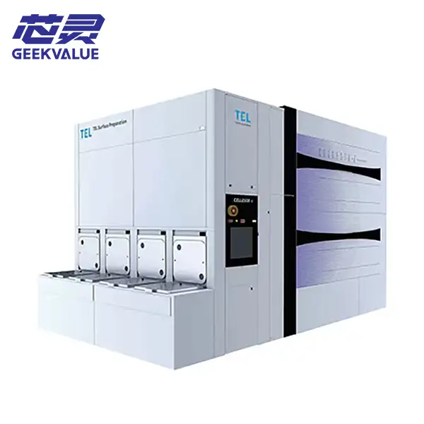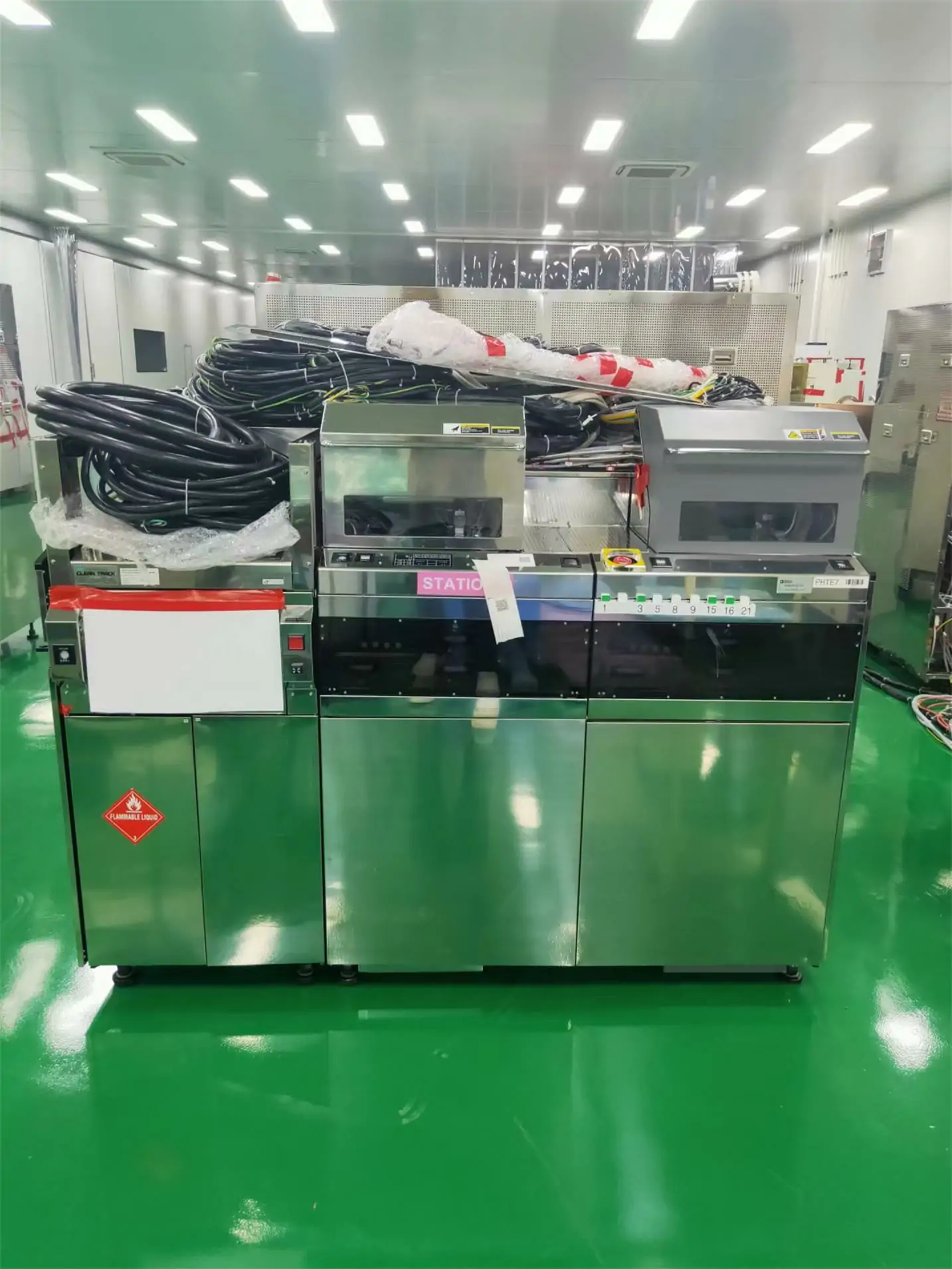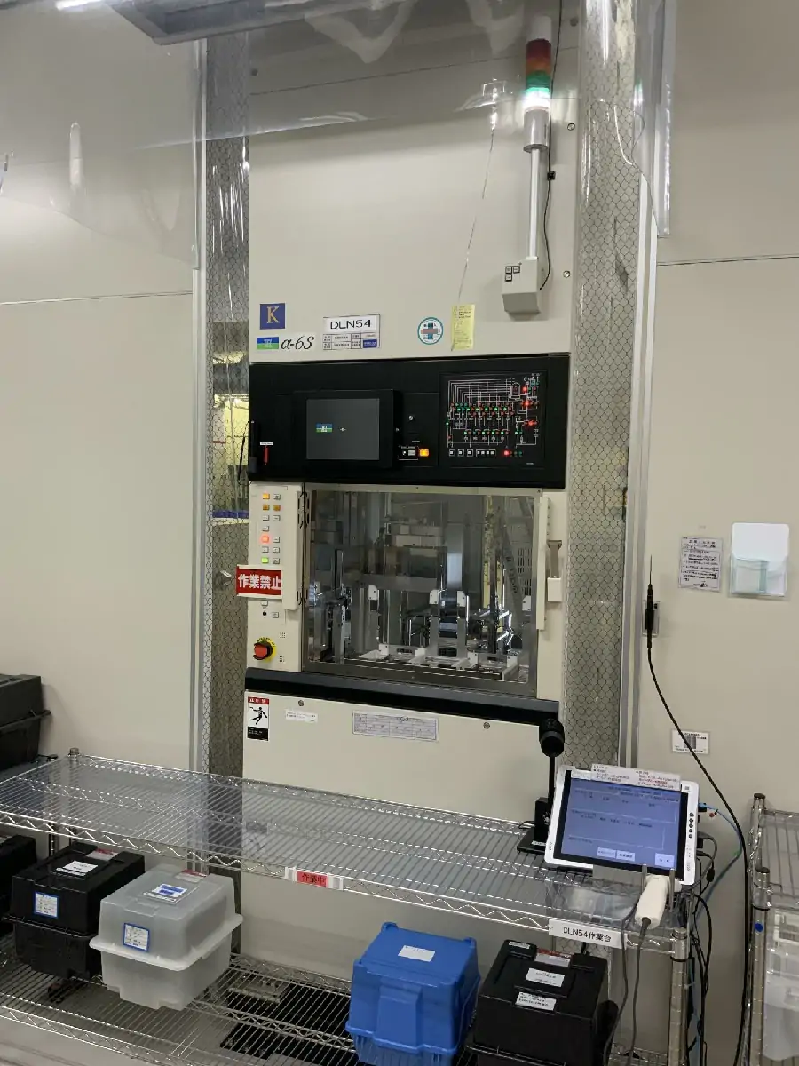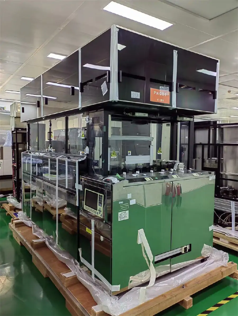
A proven lithography track from TEL, the MARK 8 is an integrated coater & developer built for 200mm wafer photoresist processing. It combines photoresist coating, thermal bake, and post-exposure developing in one continuous sequence to support mature-node patterning.
Modular station layout gives great flexibility for process tuning. Precise spin speed and temperature control maintain consistent photoresist film thickness, while integrated edge bead removal reduces defects at wafer edges.
Many fabs rely on this platform for stable daily throughput. Its mature mechanical design lowers unexpected downtime, making it a dependable addition when expanding lithography capacity.

TEL MARK 8 Main Specifications
| Manufacturer | Tokyo Electron Limited |
|---|---|
| Brand | TEL |
| Model | MARK 8 |
| Equipment Type | Wafer Coater and Developer Track System |
| Supported Wafer Sizes | 6-inch and 8-inch wafers, according to the available listing |
| Listed Process Configuration | 2C+2D; actual installed modules must be confirmed |
| Primary Process | Photoresist coating and developing |
| Condition | Used semiconductor equipment |
| Availability | Subject to current stock and configuration confirmation |