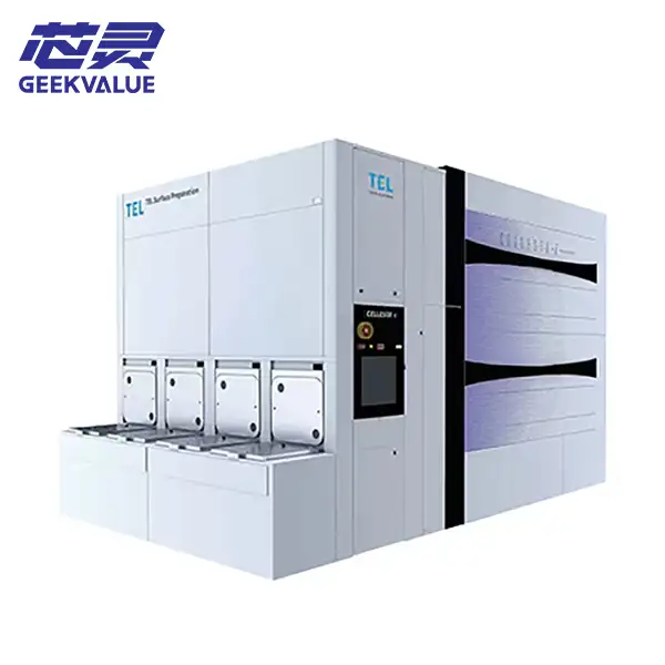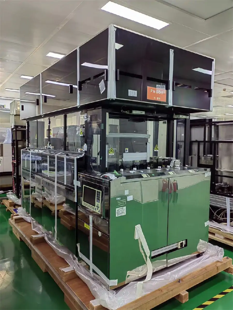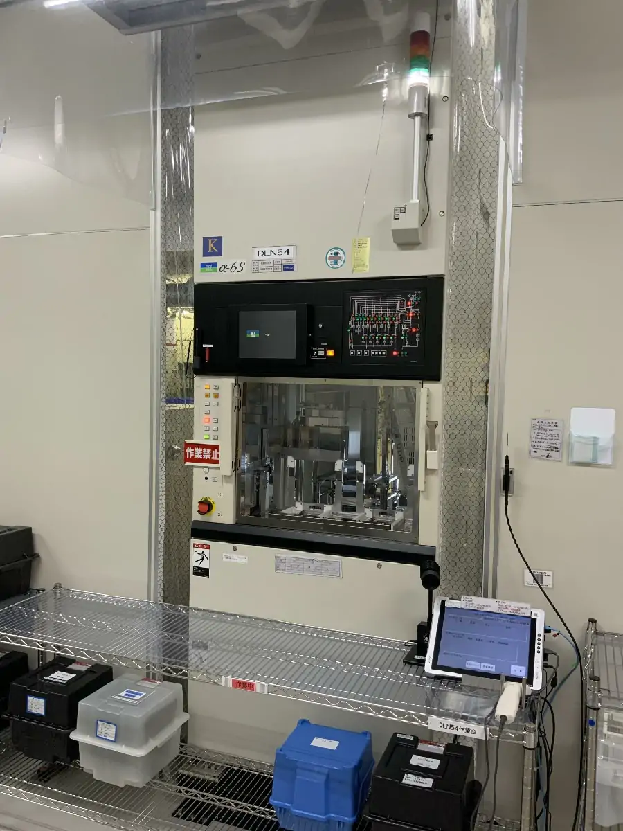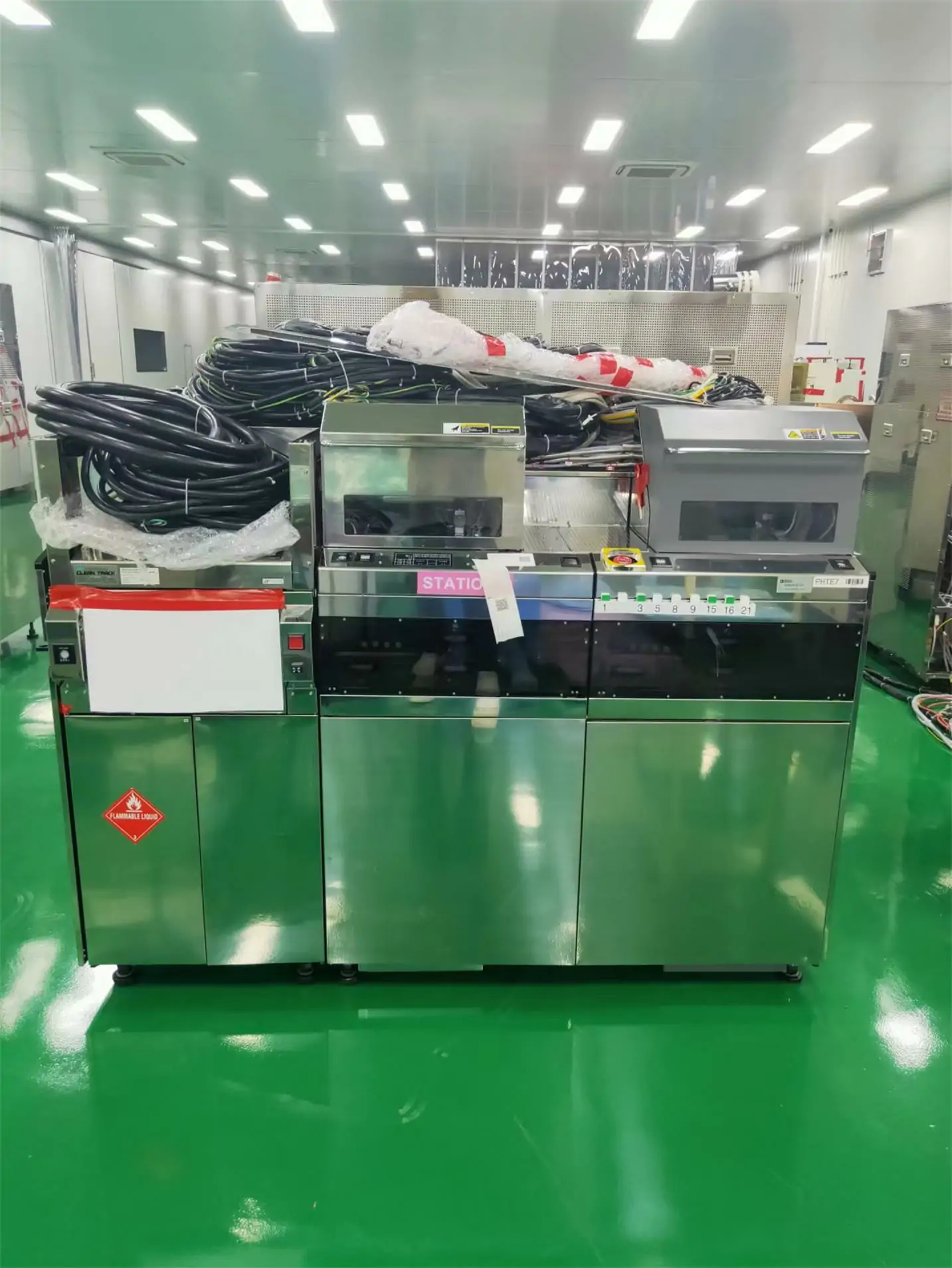
As a high-performance lithography track, the TEL MARK Vz integrated coater & developer handles 200mm wafer photoresist processing for mass production lines. It seamlessly links HMDS priming, resist spin coating, baking and pattern developing within a single automated platform.
Optimized fluid delivery and temperature management keep tight control over photoresist uniformity across the wafer surface. Advanced edge bead removal and environmental isolation work together to suppress particle generation and reduce patterning defects.
Engineered for long continuous operation, this track balances high throughput with easy preventive maintenance. It is widely adopted in power device and discrete semiconductor fabs to sustain stable lithography output.

TEL MARK Vz Main Specifications
| Manufacturer | Tokyo Electron Limited |
|---|---|
| Brand | TEL |
| Model | MARK Vz |
| Equipment Type | Wafer Coater and Developer Track System |
| Supported Wafer Size | 6-inch wafers, according to the available listing |
| Listed Process Configuration | 2C and 2D; actual installed modules must be confirmed |
| Primary Process | Photoresist coating and developing |
| Condition | Used semiconductor equipment |
| Availability | Subject to current stock and configuration confirmation |