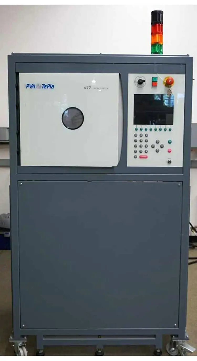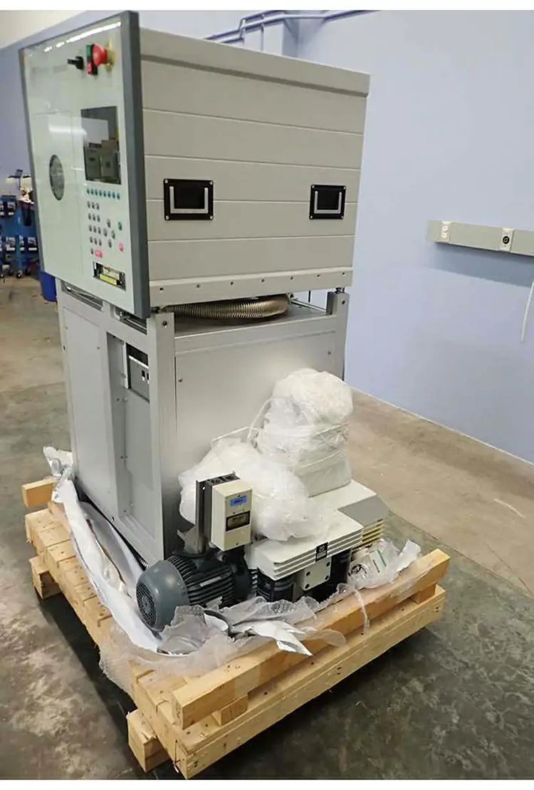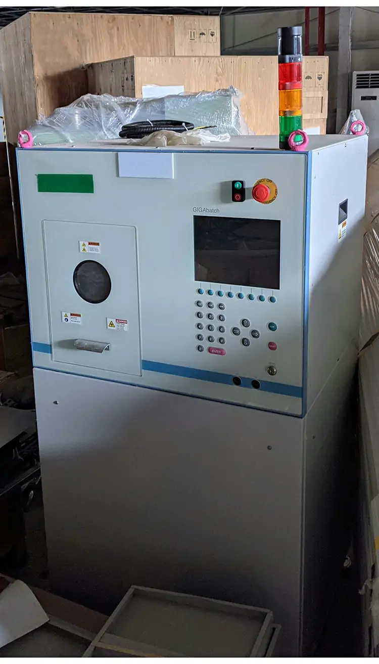
The PVA TePla / Technics GIGAbatch 360M uses electrode-less 2.45 GHz microwave plasma technology to remove photoresist and polymer residues from 150 mm and 200 mm semiconductor wafers. The process is relevant to power semiconductor and discrete device manufacturing, where clean wafer surfaces are needed before subsequent fabrication steps.
Unlike electrode-based plasma systems, microwave plasma generation avoids direct electrode contact with the process environment. Adjustable gas flow and chamber pressure allow process conditions to be tailored to different residue removal and surface treatment requirements. Batch processing also enables multiple wafers to be treated in a single run.
When purchasing a used GIGAbatch 360M, check the chamber configuration, wafer handling system, process control functions and operating status against the requirements of the intended production line.
PVA TePla GIGAbatch 360M Main Specifications
| Manufacturer | PVA TePla / Technics |
|---|---|
| Model | GIGAbatch 360M |
| Equipment Type | Microwave Plasma Batch Asher and Wafer Cleaning System |
| Plasma Frequency | 2.45 GHz |
| Microwave Power | 0–1,000 W |
| Vacuum Chamber Material | Quartz |
| Chamber Diameter | 245 mm |
| Chamber Depth | 395 mm |
| Chamber Volume | 18 L |
| Wafer Capacity | Up to 50 wafers with a diameter of 150 mm, depending on the installed wafer carrier |
| Process Gas Control | Two MFC-controlled gas lines in the base platform configuration |
| Process Monitoring | Wafer temperature monitoring and endpoint detection in the base platform configuration |
| Electrical Connection | 230 V, 15 A, 50/60 Hz |
| Approximate Dimensions | 795 × 1,540 × 710 mm |
| Approximate Weight | 190 kg |
| Equipment Year | 2013, according to the available equipment listing |
| Condition | Used semiconductor equipment |
| Availability | Subject to current stock, inspection and configuration confirmation |