Wafer Test · Repair & Refurbishment
Probe Card Repair
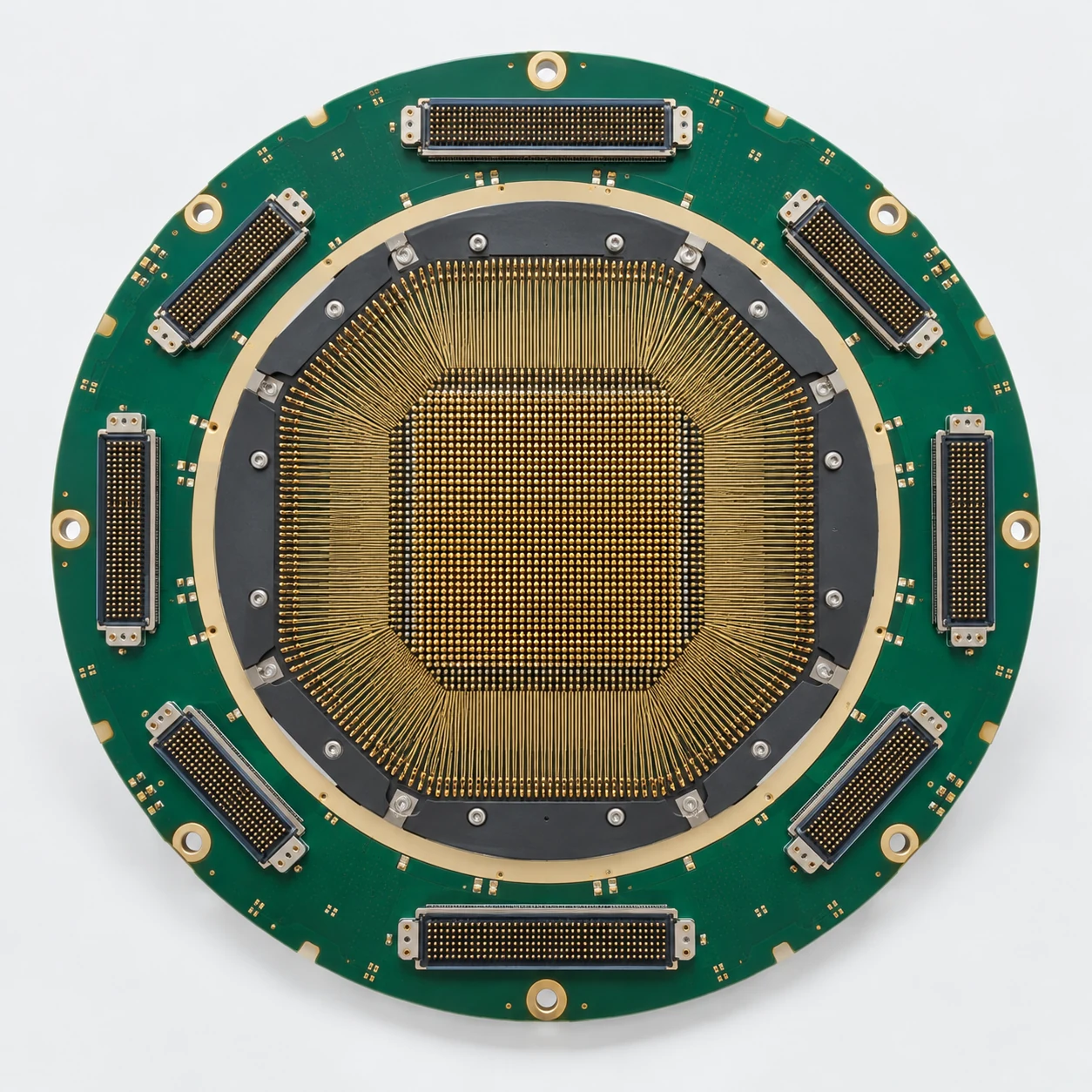
Unstable contact is costing test time. GK-SEMI repairs and refurbishes semiconductor probe cards affected by worn tips, poor contact and alignment issues. Recover a viable original card before committing to a costly replacement.
Send the card identification, test symptom and a photo of the contact area to get started.
What We Repair
Probe Card Repair Services
Repeat touchdowns, rising contact resistance and localized test failures can make a serviceable card look unusable. We focus repair work on the affected contacts and the card's actual construction, instead of treating every failure as a reason to replace the complete assembly.
Contact Cleaning & Recovery
Address oxidation, debris and contact contamination linked to intermittent opens, repeated re-probe and increased contact resistance. Cleaning and reconditioning methods are selected for the probe material and card design.
Probe Tips & Alignment
Inspect worn, bent or displaced tips; assess reshaping, needle replacement or localized realignment where the card permits. Review tip geometry, X/Y position and Z-planarity against the application instead of applying one adjustment to every card.
Electrical & Return Checks
Investigate continuity, contact resistance (Cres) and relevant electrical paths. After approved rework, communicate the inspection and bench checks completed, plus any scrub-mark or contact confirmation that belongs on the customer's wafer-test setup.
Why Work With Us
Keep the Original Card
A new card has to fit the wafer, tester interface and installed test setup. Repairing the original can help preserve that match while addressing the actual contact failure.
Work Around the Failure
We begin with the failing contact pattern, test symptoms and the condition of the existing card. This helps separate card damage from prober alignment or other test-cell issues before a repair path is agreed.
Preserve the Working Setup
Targeted rework aims to recover useful contacts without needlessly changing the card interface, pad pattern or operating configuration. The repair scope is aligned to what the card design can safely support.
Repair or Find a Match
When damage makes recovery impractical, our parts-sourcing route keeps the next step moving. Replacement matching considers the card type, device pad layout, tester connection and application, not appearance alone.
Working on the wider test setup? Explore Probe Station Board Repair, ATE Board Repair or semiconductor parts sourcing.
From Fault to Decision
How Repair Moves Forward
We keep the assessment focused on the reported failure and the actual probe-card design. The agreed checks distinguish work completed on the card from final confirmation on a wafer tester.
Identify the Card
Review the part number, card type, test application and failure pattern.
Inspect the Contacts
Review visible tip wear, contamination, alignment and substrate condition.
Agree the Scope
Define feasible rework, required checks and limitations for that card construction.
Carry Out Repair
Complete approved cleaning, localized tip work or alignment correction.
Review the Result
Check relevant contact geometry, continuity and Cres where measurable.
Return to Test
Report the bench-work boundary and the on-tool checks needed after refit.
Repair Experience
Contact Stability, Restored
A vertical probe card with localized contact failures illustrates why card-level inspection can change a replacement decision.
A Vertical Card Returned to Test
The problem. A wafer-test line saw a sharp increase in contact failures on a vertical probe card. Replacing the assembly was being considered, with a lengthy OEM supply window.
What inspection found. The observed fault was concentrated in one region. Localized oxidation and a modest planarity deviation were identified, rather than a failure requiring replacement of the complete card.
Repair and outcome. The affected contacts were cleaned and the relevant planarity condition corrected. Contact behavior stabilized and the original card returned to production, avoiding an immediate full-card replacement.
Verification boundary. Card-level checks informed the repair decision; final contact performance was established in the installed wafer-test application.
Based on a repair experience. The outcome and lead time relate to this card and test setup.
Common Questions
Probe Card Repair FAQs
Practical answers on card types, contact issues, return checks and replacement options.
Can you repair bent or broken probe needles?
Some cantilever designs allow localized straightening or needle replacement. Vertical and MEMS structures can have different limits. We review the actual construction and extent of damage before proposing a method.
Will cleaning solve repeated re-probe failures?
Only if contamination is responsible. Worn tips, planarity, prober alignment and test conditions can produce similar symptoms. Share the failure pattern so the right cause is investigated.
Can reshaping change the scrub mark?
Yes. Tip geometry, position and overtravel affect scrub behavior. Where reshaping is appropriate, the work should respect the relevant pad dimensions and contact requirements, with final scrub confirmation on the customer's setup.
How do you check a probe card after repair?
Checks depend on the card and agreed scope. They may include visual condition, position, continuity and contact resistance. Final wafer-test yield and scrub performance require confirmation under the installed test conditions.
Is every vertical or MEMS probe card repairable?
No. Some structures have restricted repair paths, and damage to the probe array or substrate may make replacement more appropriate. We assess the card design rather than promise universal coverage.
What if the original card cannot be recovered?
We can discuss sourcing a matching replacement. Provide the card identity, tester interface, device pad layout and test application to narrow suitable options.
Do you support discontinued probe cards?
Legacy cards can still be assessed for practical repair. Where parts or a complete replacement are needed, availability and compatibility are checked against the specific card.
What should I send for a repair enquiry?
Start with the model or part number, a clear card and tip-area photo, the tester or prober application, and the contact problem observed. Test data helps, but is not required for the first discussion.
Talk to Our Repair Team
Recover Your Probe Card
Tell us where contact is failing and which card is installed. Our team can discuss a targeted repair route, the relevant checks and a matching replacement option when repair is not practical.
Request Probe Card Support ↗