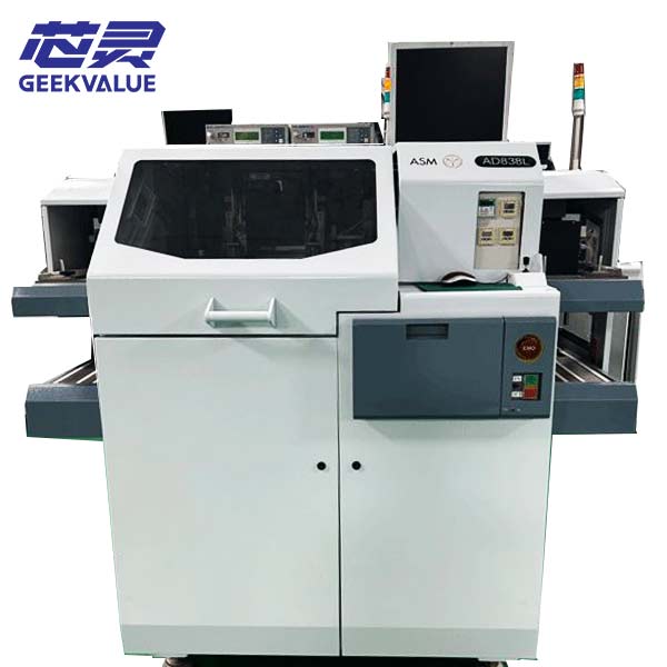
ASMPT AD838L automatic die bonder delivers stable high-throughput die attach and flip chip processing. Its core architecture builds on three integrated subsystems: dynamic vision alignment, optimized bond head actuation, and low-drag substrate material handling. The design balances placement repeatability and continuous output while maintaining yield on fragile panels.
Core Technologies of the ASMPT AD838L Automatic Die Bonder
Dynamic On-the-Fly Vision Alignment
The up-looking PR on-the-fly vision engine completes pattern recognition as the stage keeps moving, eliminating idle waiting time within each bonding cycle. Real-time visual feedback dynamically offsets positional deviation, sustaining XY placement precision up to ±15μm @3σ for large-format substrates up to 300 mm × 100 mm. This vision framework accommodates varied die geometries and substrate patterns and simplifies recipe switching between different packaging lots.
Tunable Bond Head Actuation & Force Regulation
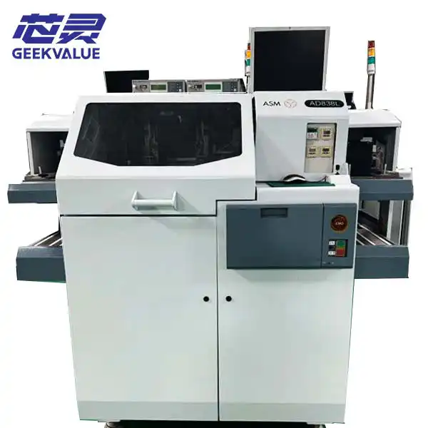
Patented bond head mechanics refine force control and pickup-release motion sequences. The actuator holds consistent bonding force across silver paste, epoxy and DAF die attach film, supporting standard die attach and flip chip interconnection. Tunable bonding parameters reduce mechanical stress on ultra-thin and brittle chips and cut chip cracking incidents during high-volume runs.
Low-Vibration Substrate Transport System
The proprietary drag-free indexing system transports large and sensitive substrates without surface scratching. The material transport path suppresses substrate vibration during indexing and protects surface integrity of easily damaged optical components. Optional auto wafer loading modules connect with upstream and downstream factory automation, lowering manual intervention and production downtime.
Process Monitoring and Factory Automation Compatibility
The platform maintains continuous operation over extended manufacturing shifts, with embedded process logging and real-time status tracking. Operators modify bonding recipes, vision parameters and handling routines through a streamlined HMI. It runs reliably within mid-to-high volume packaging environments, handling LED, optical sensor and discrete semiconductor device assembly.