BGA and flip chip packaging are related semiconductor packaging concepts, but they describe different aspects of a package. BGA, or Ball Grid Array, describes an external connection structure that uses an array of solder balls to connect a package to a printed circuit board. Flip chip describes a method of connecting a semiconductor die to a substrate with the die's active surface facing downward.
The two terms are not mutually exclusive. A package can use flip chip bonding inside the package and a BGA interface to connect the completed package to a circuit board. This combination is commonly known as flip chip BGA, or FC-BGA.
Understanding the distinction helps engineers compare package architectures, evaluate electrical and thermal requirements, and select suitable assembly equipment. It also prevents a common misunderstanding: BGA is not simply another name for flip chip bonding, and flip chip does not automatically mean that the finished package uses a ball grid array.
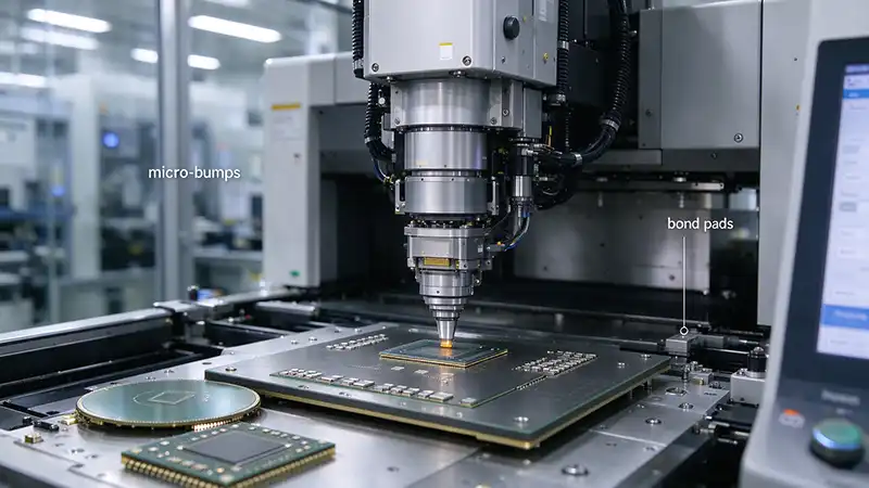
What Is BGA Packaging?
BGA stands for Ball Grid Array. It is a semiconductor package format in which solder balls are arranged in a grid on the underside of the package. During board assembly, these balls connect the package's external terminals to matching pads on a printed circuit board, usually through a soldering process.
The solder balls provide electrical connections and help establish the mechanical attachment between the package and the circuit board. Their arrangement can support a substantial number of external connections within a relatively compact footprint.
BGA is an external package-to-board connection method. It does not, by itself, specify how the semiconductor die is connected inside the package. Depending on the design, the die inside a BGA package may be connected by wire bonding, flip chip bonding, or another suitable interconnection approach.
How Does BGA Packaging Work?
The BGA assembly flow varies by package type, but a typical process includes die attachment, electrical interconnection, package formation, external terminal preparation, and board-level mounting.
First, the semiconductor die is attached to a package substrate or lead structure. The internal connection is then established. In a wire-bonded package, fine wires connect the die pads to substrate contacts. In a flip chip package, conductive bumps or pillars connect the die to corresponding substrate contacts.
The package is then completed through the required encapsulation, molding, or other assembly operations. Solder balls are formed or attached to the external contact pads on the package underside. After inspection and testing, the package can be mounted on a printed circuit board using a compatible surface-mount process.
The exact order of these operations depends on the package design. Not every BGA package uses the same internal die connection, substrate structure, or assembly flow.
What Are the Main Characteristics of BGA?
BGA packages distribute external connections across an array of solder balls rather than relying exclusively on terminals around the package perimeter. This can support a higher number of external connections within a given footprint.
The ball grid also provides a practical interface for automated surface-mount assembly. However, successful board-level attachment depends on pad design, solder paste printing, component placement, reflow conditions, board warpage, and inspection.
BGA solder joints are located underneath the package after mounting, so visual inspection from above cannot reveal every connection defect. X-ray inspection and electrical testing are commonly used when the assembly requirements call for additional verification.
What Is Flip Chip Packaging?
Flip chip packaging uses a die orientation in which the active surface faces the substrate. Electrical connections are made through conductive bumps, copper pillars, or other interconnect structures placed between the die and substrate.
Compared with conventional wire bonding, this arrangement can distribute connections across much of the die surface. It can also shorten the electrical path between the die and package substrate, depending on the complete package layout.
Flip chip describes the internal die-to-substrate interconnection approach. It does not necessarily determine the external terminal style of the finished package. A flip chip device may use a BGA interface, but other package configurations are possible.
How Does Flip Chip Packaging Work?
The die must have a suitable interconnect structure, such as solder bumps or copper pillars, and the substrate must contain matching contact locations. The die is placed face-down and aligned so that its terminals correspond to the substrate pads.
A suitable bonding process then forms the connections. Solder reflow and thermocompression bonding are common options, although the actual method depends on the interconnect materials and package design.
After bonding, the assembly may receive underfill or another form of mechanical reinforcement where required. The package then proceeds through the remaining manufacturing, inspection, and testing stages.
The alignment and bonding requirements can be demanding, particularly when the contact pitch is small or the die has a high number of interconnections. Process parameters must be matched to the bump structure, substrate, materials, and required reliability.
What Are the Main Characteristics of Flip Chip?
Flip chip assembly can support high interconnect density because contacts do not need to be confined to the perimeter of the die. This is useful for devices with many input/output connections or demanding electrical requirements.
The absence of conventional wire loops can also help reduce package height and interconnection length. However, these benefits depend on the complete package design. Flip chip bonding alone does not guarantee a smaller package, lower operating temperature, or better electrical performance in every application.
The approach also creates manufacturing challenges. Fine-pitch placement requires accurate alignment, hidden joints may need specialized inspection, and the materials must tolerate the mechanical and thermal conditions encountered during assembly and operation.
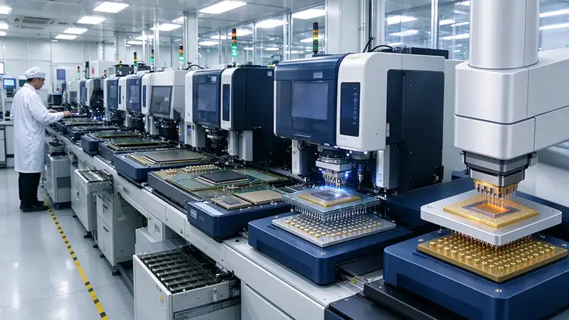
BGA vs. Flip Chip: What Is the Difference?
The key difference is the level of the package being described. BGA concerns how the package connects to the circuit board. Flip chip concerns how the die connects to the substrate inside the package.
| Comparison point | BGA packaging | Flip chip packaging |
|---|---|---|
| Meaning | Ball Grid Array external package connection format | Die-to-substrate interconnection approach |
| Main connection | Package terminals to printed circuit board | Semiconductor die to substrate or another component |
| Typical structure | Array of solder balls on the package underside | Bumps, pillars, or other conductive interconnects beneath the die |
| Die orientation during internal attachment | Depends on the internal assembly method | Active surface faces the substrate |
| Internal die connection | May use wire bonding or flip chip bonding | Uses flip chip-style direct interconnections |
| Main design consideration | External connection layout and board assembly | Die alignment, interconnect density, and bonding process |
| Inspection concerns | Hidden solder joints beneath the mounted package | Hidden die-to-substrate joints beneath the die |
| Can they be combined? | Yes | Yes; FC-BGA is a common combined package concept |
The terms answer different questions. If an engineer asks how a package connects to the motherboard, BGA may be the relevant term. If the question concerns how the silicon die connects to the package substrate, flip chip may be the more relevant term.
What Is FC-BGA?
FC-BGA stands for Flip Chip Ball Grid Array. It combines flip chip die attachment inside the package with a ball grid array for the external connection to the printed circuit board.
In a typical FC-BGA structure, the semiconductor die is mounted face-down onto a package substrate through an array of bumps or pillars. The substrate routes the electrical connections to external solder balls located on its underside. Those balls connect the package to the circuit board during board-level assembly.
This architecture can support devices with high interconnect requirements, including certain processors, graphics devices, networking components, and other complex semiconductor products. The exact package design depends on the die, substrate, routing requirements, power delivery, signal integrity, and thermal solution.
FC-BGA is not a separate alternative to flip chip in the same sense that wire bonding is an alternative internal interconnection method. It is a package configuration that combines an internal bonding approach with an external terminal format.
How Is FC-BGA Different from a Wire-Bonded BGA?
A wire-bonded BGA connects the die to the substrate using fine metal wires. The die is commonly attached with its active surface facing upward, and wires run between die pads and substrate contacts.
An FC-BGA uses flip chip interconnections to connect the die directly to the substrate. This can shorten the internal connection paths and allow contacts to be distributed across the die surface.
Both package types may use a ball grid array to connect to the printed circuit board. Their differences lie mainly in the internal connection structure, package layout, process requirements, and resulting electrical and mechanical characteristics.
The choice is not determined by a single performance metric. Designers must consider cost, die size, pin count, signal requirements, thermal behavior, substrate design, production capability, and qualification requirements.
Electrical Performance: BGA vs. Flip Chip
Electrical performance depends on the entire interconnection path, including the die, package substrate, external terminals, circuit board, and operating environment.
Flip chip structures can reduce the length of the internal die-to-substrate connections compared with many wire-bonded designs. Shorter interconnections can help control parasitic inductance and support demanding signal requirements. The benefit is particularly relevant when package-level interconnect effects become significant.
BGA, by contrast, describes the external connection arrangement. The ball grid provides connections between the package and board, but the term alone does not establish the electrical performance of the package. Ball pitch, package routing, substrate construction, board layout, and signal assignment all affect the final result.
It is therefore misleading to say that flip chip is always electrically superior to BGA. A more accurate comparison distinguishes internal die interconnection from external package-to-board attachment.
Thermal Performance: Which Is Better?
Thermal behavior depends on the complete package architecture rather than the name of the interconnection method alone.
Flip chip packages may provide useful heat-transfer paths through the die interconnects and substrate, depending on their design. Some packages also use heat spreaders, lids, thermal interface materials, or other cooling structures. The thermal result depends on the materials, geometry, power density, and cooling system.
BGA packages can be designed for a wide range of thermal conditions. Their performance depends on package construction, board design, thermal vias, copper distribution, heat spreaders, and the way heat is removed from the device.
A package intended for a high-power processor has different thermal requirements from a low-power controller, even if both use BGA terminals. Engineers should evaluate junction temperature, thermal resistance, power dissipation, and the actual cooling arrangement instead of selecting a package based only on its category.
Package Size and Interconnect Density
BGA can provide many external connections in a compact package footprint because solder balls are arranged in a grid. The achievable connection count depends on ball pitch, package dimensions, routing layers, and design rules.
Flip chip bonding can support dense connections between the die and substrate because the interconnects may extend across much of the die surface. This is useful when a device requires a large number of internal connections.
In FC-BGA, the two structures serve different purposes: the flip chip interconnects connect the die to the substrate, while the BGA terminals connect the package to the circuit board.
The finished package size still depends on many other factors, including die dimensions, substrate routing, power delivery, mechanical support, and thermal management. Neither BGA nor flip chip should be treated as a universal guarantee of the smallest possible package.
Manufacturing Complexity and Cost
The manufacturing cost of a package reflects materials, equipment, production volume, yield, inspection, process control, and qualification requirements.
BGA assembly requires reliable external terminal formation and board-level soldering. Fine-pitch or high-density BGA designs may need careful control of solder paste, placement, reflow, warpage, and inspection. Rework can be challenging because the solder joints are hidden beneath the package.
Flip chip assembly adds requirements associated with die-side interconnects, precise alignment, and bonding. Depending on the package, bump formation, substrate preparation, underfill, and specialized inspection can add process steps and cost.
A flip chip BGA package may offer advantages that justify its additional process complexity in some applications. In others, a wire-bonded package or a different package format may provide a more economical solution. Cost comparisons should use the complete manufacturing flow and the intended performance requirements rather than focusing on a single assembly operation.
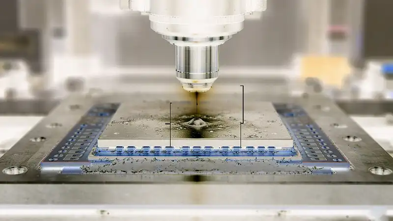
Common Applications of BGA and Flip Chip Packaging
Applications of BGA
BGA is used in many semiconductor products that require a practical external connection interface with a relatively high terminal count. Examples can include processors, memory devices, controllers, communication components, and consumer electronics.
The specific BGA variant depends on the package size, terminal pitch, thermal requirements, board constraints, and electrical needs. The presence of a BGA interface does not reveal whether the internal die connection uses wires or flip chip interconnects.
Applications of Flip Chip
Flip chip technology is used where direct die-to-substrate connections provide useful benefits. Applications may include high-performance computing, advanced processors, graphics devices, networking components, and certain radio-frequency or specialized semiconductor products.
The exact choice depends on interconnect density, signal requirements, power, thermal design, package size, and the manufacturing process available to the product team.
Applications of FC-BGA
FC-BGA combines the internal connection characteristics of flip chip with the external connection arrangement of BGA. It is used in some complex devices that require dense die-to-substrate connections and a package interface suitable for board-level assembly.
The architecture is not required for every high-performance device. It is selected when its electrical, mechanical, thermal, and manufacturing characteristics fit the product requirements.
How Do Engineers Choose Between BGA and Flip Chip?
The first step is to clarify which design decision is being made. BGA is an external terminal format, whereas flip chip is an internal interconnection method. An engineer may need to select a package format, an internal bonding process, or a combination of both.
Important factors include:
Input/output requirements: Determine the number and distribution of required connections.
Signal integrity: Evaluate interconnection length, parasitic effects, operating frequency, and routing.
Thermal requirements: Consider power dissipation, heat-transfer paths, and cooling constraints.
Package dimensions: Assess the required footprint, height, and mechanical envelope.
Manufacturing capability: Confirm access to suitable die attachment, bonding, inspection, and board assembly processes.
Reliability targets: Evaluate thermal cycling, mechanical stress, moisture exposure, and other relevant conditions.
Cost and yield: Compare the full manufacturing process, material cost, production volume, and expected defect rate.
These factors should be considered together. A package that performs well electrically may be less attractive if it requires unavailable manufacturing capability or creates unacceptable production cost.
Frequently Asked Questions
Is BGA the same as flip chip?
No. BGA describes the external package connection format, using an array of solder balls to connect the package to a circuit board. Flip chip describes how the die is connected to the substrate inside the package.
Can a BGA package use wire bonding?
Yes. A BGA package may use wire bonding or flip chip bonding for the internal die connection. The BGA designation alone does not determine the internal interconnection method.
Is FC-BGA a type of flip chip packaging?
FC-BGA is a package configuration that combines flip chip die-to-substrate interconnection with BGA terminals for package-to-board connection.
Does flip chip always offer better performance than BGA?
This comparison is not technically direct because the terms describe different parts of the package. Flip chip may shorten internal interconnections, while BGA defines the external connection arrangement. Overall performance depends on the full package and board design.
Which is cheaper: BGA or flip chip?
There is no universal answer. BGA describes the external terminal format, while flip chip describes an internal bonding approach. Cost depends on the specific package, materials, production volume, equipment, yield, inspection, and qualification requirements.
Is flip chip used only in high-performance processors?
No. Flip chip is used in several types of semiconductor products. Its suitability depends on the interconnection density, package design, electrical requirements, and manufacturing economics.
Conclusion
BGA and flip chip packaging are related but distinct concepts. BGA defines how a package connects to a printed circuit board through an array of solder balls. Flip chip defines how a die connects to a substrate through conductive bumps, pillars, or similar interconnects.
FC-BGA combines both: flip chip bonding forms the internal die-to-substrate connections, and solder balls provide the external package-to-board interface. This distinction is essential when comparing package designs, discussing equipment requirements, or evaluating semiconductor assembly processes.