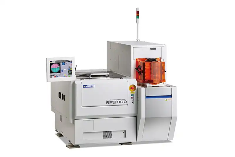
A wafer prober is a semiconductor test platform that positions a wafer and establishes electrical contact with selected devices or test structures. Working with a probe card or other probing interface and electrical test instruments, it enables engineers to evaluate chips before the wafer is diced into individual dies.
The equipment is used in semiconductor research, process development, wafer sort, and production testing. Its role is different from that of an automatic test system: the prober handles positioning and contact, while the connected tester performs electrical measurements.
Choosing a wafer prober requires more than checking its wafer diameter or automation level. The intended test, contact geometry, measurement environment, software, and interface compatibility all influence whether a machine can perform the required task.
What Does a Wafer Prober Actually Do?
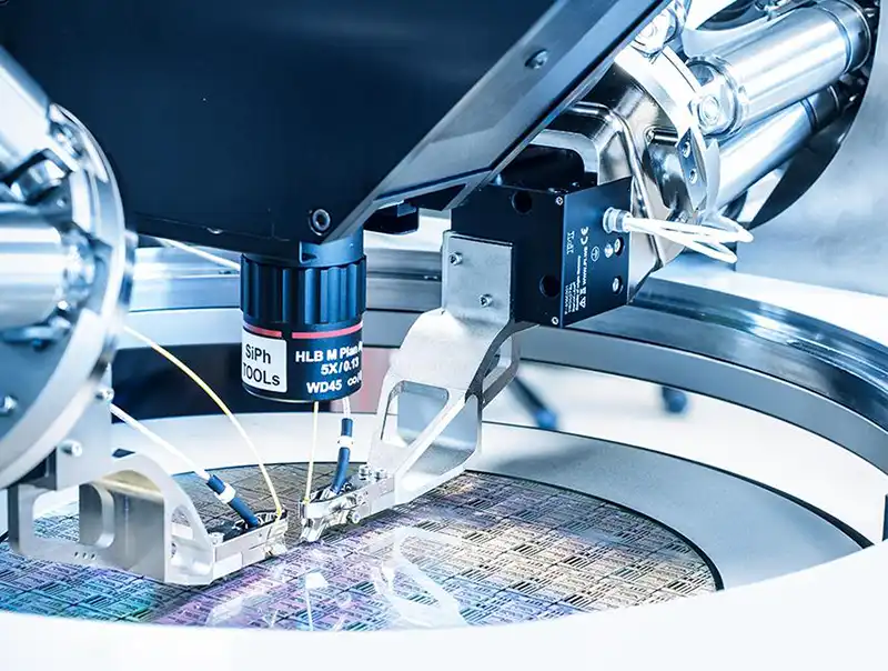
The most important function of a wafer prober is to bring the correct area of a wafer into repeatable contact with the probing interface.
A wafer contains many individual dies or test structures. Each target must be positioned accurately enough for the probe tips to reach the intended electrical pads. After contact is established, a connected tester applies signals and measures the device response.
The resulting data may help engineers determine whether a device meets specified electrical limits, investigate process variations, or identify dies that require further analysis.
A typical test sequence includes wafer loading, alignment, positioning, probe contact, electrical measurement, and movement to the next test location. Fully automatic systems may coordinate much of this sequence without requiring the operator to reposition each die manually.
However, not every wafer prober is intended for high-volume production. Some systems are better suited to laboratory characterization, where measurement flexibility and electrical stability matter more than wafer throughput.
Wafer Prober Applications: Research vs. Production
Wafer Probers for Research and Development
In semiconductor R&D, engineers may need to measure prototype devices, investigate process changes, or characterize electrical structures before a manufacturing process is finalized.
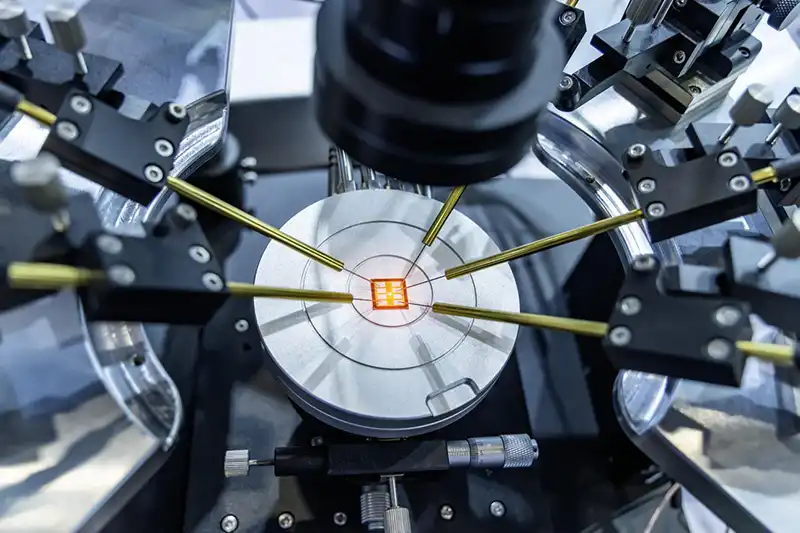
These tasks can require flexible probe positioning, low-noise measurements, specialized instruments, and temperature-controlled testing. A manual or semi-automatic prober may be suitable when test locations change frequently or only selected structures need to be measured.
For low-current measurements, electrical shielding, grounding, leakage control, and environmental stability can be as important as the mechanical positioning system.
Wafer Probers for Production Testing
Production wafer probing has different priorities. The equipment may need to handle wafers repeatedly, follow a programmed test sequence, communicate with automatic test equipment, and maintain consistent contact across many dies.
Throughput depends on more than stage speed. Alignment time, probe-card design, test duration, the number of sites contacted per touchdown, and wafer handling can all affect overall productivity.
A machine with extensive automation is not automatically the best choice if it cannot support the required test interface or device layout.
Which Wafer Prober Specifications Matter Most?
The specifications that matter depend on the intended application.
| Selection factor | Why it matters |
|---|---|
| Wafer diameter and handling | The machine must accommodate the required wafer format and handling process |
| Positioning accuracy and repeatability | Probe tips must reach the intended contact pads consistently |
| Probe-card compatibility | The interface must match the device layout and electrical test setup |
| Tester integration | Communication, cabling, and interface hardware must support the test system |
| Temperature capability | Thermal testing requires suitable chuck and temperature-control options |
| Electrical environment | Low-current and high-frequency tests may require specialized shielding or interfaces |
| Automation | The operating mode should match engineering or production requirements |
| Software and data handling | Alignment routines, wafer maps, and test interfaces must support the workflow |
A specification sheet should be reviewed in the context of the target application. For example, a system intended for low-current transistor characterization may have different requirements from one used for automated production wafer sort.
Why Wafer Size Alone Is Not Enough
Wafer diameter is an important starting point, but it does not establish complete equipment compatibility.
A machine that accepts the correct wafer size may still lack the required probe card, thermal configuration, tester interface, software option, or handling capability.
The physical condition of the wafer chuck and motion stage also matters. Wear, vibration, contamination, or inconsistent positioning can interfere with reliable contact.
Before purchasing a wafer prober, confirm the exact model and installed configuration rather than relying only on a general product description.
What Should You Check Before Buying a Used Wafer Prober?
Used equipment can provide a practical option for engineering laboratories, mature-process production, or facilities expanding existing test capacity. Its suitability depends on the actual machine condition and the compatibility of its configuration.
A useful evaluation should cover:
Mechanical condition: Check stage movement, chuck condition, alignment behavior, and visible wear.
Functional operation: Review alarms, wafer handling, control software, and supported operating sequences.
Test compatibility: Confirm the probe-card arrangement, tester connections, interface hardware, and required options.
Application requirements: Verify wafer format, contact geometry, temperature capability, and measurement needs.
Documentation: Request available maintenance records, configuration details, manuals, and service information.
Accessories and support: Establish which accessories are included and whether replacement parts or technical support are available.
A demonstration using a representative wafer or test setup can reveal problems that a specification list cannot. If a machine is supplied without a probe card or tester, those missing items should be accounted for when evaluating the total cost and implementation effort.
Wafer Prober vs. Probe Station
The terminology overlaps across manufacturers and applications.
A wafer prober commonly refers to a system that positions wafers for semiconductor testing, including automated wafer sort. A probe station is often associated with laboratory measurements and may provide flexible access to individual devices or test structures.
Neither term guarantees a particular level of automation. Manual, semi-automatic, and automatic systems exist across the broader probing equipment category.
The correct comparison should focus on wafer handling, positioning, electrical interfaces, measurement requirements, and the intended workflow.
Frequently Asked Questions
What is the main purpose of a wafer prober?
Its main purpose is to position a wafer and establish electrical contact with selected devices or test structures so that connected instruments can measure their electrical characteristics.
Does a wafer prober perform the electrical test itself?
Not necessarily. The prober provides the mechanical positioning and contact interface. Electrical measurements are generally performed by connected test instruments or automatic test equipment.
Can a wafer prober be used for both R&D and production?
Some systems can support multiple types of work, but suitability depends on their configuration, measurement environment, automation, and compatibility with the intended devices.
What determines the price of a used wafer prober?
Model, configuration, wafer size, condition, automation, thermal options, software, accessories, and serviceability can all affect value. A reliable assessment should consider the complete test setup rather than the machine alone.
Conclusion
A wafer prober connects semiconductor devices on a wafer to the electrical test environment. Its value depends on accurate positioning, reliable contact, suitable interfaces, and compatibility with the intended testing process.
For engineering and purchasing teams, the most useful starting point is to define the device, test method, wafer format, and required configuration. Those details provide a stronger basis for selecting a new or used wafer prober than a model name or automation label alone.