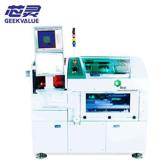
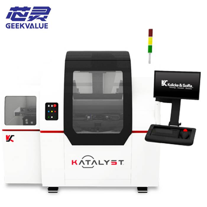
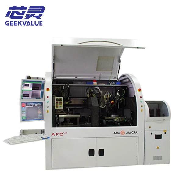
Wire bonding connects pads on a face-up die to a leadframe or substrate through fine wires. Flip chip connects a face-down die through bumps or pillars. The choice affects electrical routing, package construction, assembly flow and cost, but neither method is the best option for every device.
The practical question is whether a particular interconnect can meet the product’s electrical, mechanical and reliability requirements at an acceptable manufacturing cost. That decision starts with the die and package design.
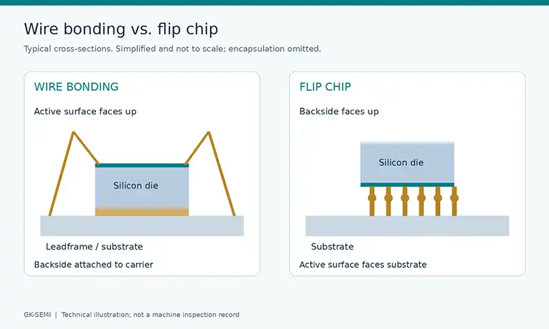
Figure 1. Typical wire-bond and flip-chip constructions. Simplified cross-sections; encapsulation is omitted.
Flip Chip and Wire Bonding at a Glance
| Consideration | Wire bonding | Flip chip |
|---|---|---|
| Die orientation | Active surface generally faces upward | Active surface faces the receiving substrate |
| Interconnect | Fine wires between die pads and package terminals | Bumps or pillars between die and substrate pads |
| Pad arrangement | Commonly near the die perimeter | Peripheral or area-array connections |
| Electrical path | Depends on wire length, loop geometry and routing | Short vertical connections can reduce interconnect parasitics |
| Die preparation | Compatible bond pads and metallurgy | Compatible bump or pillar structure |
| Assembly concerns | Bond quality, loop clearance, wire sweep and pad damage | Alignment, coplanarity, joint formation and warpage |
| Thermal performance | Depends on the complete package and cooling path | Depends on the complete package and cooling path |
| Cost basis | Die attach, wire bonding, materials, inspection and yield | Bumping, substrate, bonding, underfill where required, inspection and yield |
These differences describe common constructions. The details of a particular package still need to be checked.
What Changes in the Assembly Process?
Wire bonding separates die attachment from electrical connection
In a typical wire-bond assembly, the die is first attached to its carrier. A wire bonder then connects die pads to the package terminals.
Gold, copper, aluminum and silver-alloy wires are among the available material choices. Selection depends on pad metallurgy, package requirements, equipment capability and the qualified process.
A usable process must control more than bond placement. Loop shape, wire clearance, bond strength and interaction with later encapsulation steps all matter.
Changing products may require different tooling, wire settings, loop programs or material qualification. A program change alone does not establish that the new assembly is ready for production.
Flip chip moves the electrical interface beneath the die
In flip-chip assembly, the interconnects sit between the die’s active surface and the receiving substrate.
Depending on the technology, assembly may involve placement followed by reflow, thermocompression bonding or another qualified joining process. Underfill or related materials may also be part of the package construction.
A flip chip bonder must be evaluated against the required assembly route. Accurate placement does not, by itself, prove that the complete process can form reliable joints.
Before choosing equipment, establish who supplies the bumped die, how the joints will be formed and which subsequent operations take place elsewhere in the line.
Electrical Performance: Where the Shorter Connection Helps
Bond wires introduce electrical effects that depend on their length, shape, spacing and relationship to the surrounding package.
Flip-chip connections can shorten the path between die and substrate. This can help where interconnect inductance, power delivery or routing density limits the design.
However, shorter connections do not automatically guarantee better system performance. Substrate routing, return paths, power distribution and package transitions remain important.
Compare the two constructions against the same requirements:
Signal frequencies and rise times.
Permitted loss and coupling.
Power and ground distribution.
Current requirements.
Package routing constraints.
Wire bonding remains a viable choice for many demanding products when the package and interconnect are engineered accordingly. The comparison needs an electrical model, rather than a general assumption about which technology is more advanced.
I/O Density: Avoid a Universal Switching Threshold
Wire bonding commonly accesses pads around the die perimeter. Increasing connection counts can create restrictions involving pad pitch, wire clearance and package routing.
Flip chip can distribute connections over a larger portion of the die surface. This provides additional routing opportunities for dense signal and power connections.
There is no single I/O count at which every product must switch technologies. Feasibility depends on die dimensions, pad arrangement, assembly capability and routing rules.
Before treating flip chip as the solution to an I/O problem, confirm that the die layout and substrate support the proposed interconnect arrangement. A different connection method may also require changes to the package and its qualification plan.
Thermal Performance: Follow the Complete Heat Path
It is misleading to assign a fixed thermal advantage to either method.
In a common wire-bond package, heat can travel from the die backside through the die-attach material into a leadframe, exposed pad or substrate. The effectiveness of that path depends on the package and its connection to the board or cooling system.
A flip-chip construction may permit cooling through the exposed die backside. Heat can also travel through the interconnect and substrate structure.
A meaningful comparison identifies:
Where heat is generated.
Which surfaces connect to the cooling system.
The thermal resistance of the complete assembly.
Relevant power-cycling and temperature conditions.
Mechanical stress associated with the materials.
A package cross-section and defined cooling conditions provide more useful information than a broad claim that one bonding method runs cooler.
Which Method Costs Less?
Wire bonding can offer an economical route when the die already has compatible pads, the package is established and assembly capacity is available.
Flip chip may introduce bumping, different substrates, tighter alignment requirements and additional material or inspection steps. Those costs must be weighed against possible savings elsewhere, including package size and routing.
Compare cost per accepted package rather than the purchase price of a bonder.
| Cost area | Questions to resolve |
|---|---|
| Die preparation | Is additional wafer-level processing required? |
| Package materials | What substrate, leadframe and interconnect materials are needed? |
| Assembly | Which machines and process steps are required? |
| Inspection | How will the relevant joints be evaluated? |
| Yield | Where can assembly losses occur? |
| Qualification | What testing and engineering work is required? |
| Product changes | What changes when the die or package is revised? |
For an existing product, conversion costs can be significant even when an alternative process looks attractive in isolation.
Reliability Depends on the Construction
Wire-bond qualification may examine bond lift, heel cracking, pad damage, corrosion and wire movement during encapsulation.
Flip-chip qualification may examine joint fatigue, interfacial failures, underfill behavior, voiding and warpage.
Neither list establishes which technology is inherently more reliable. Materials, construction, process control and the operating environment determine the relevant risks.
Temperature cycling, moisture exposure, mechanical loading and power dissipation should be considered within the product’s qualification plan.
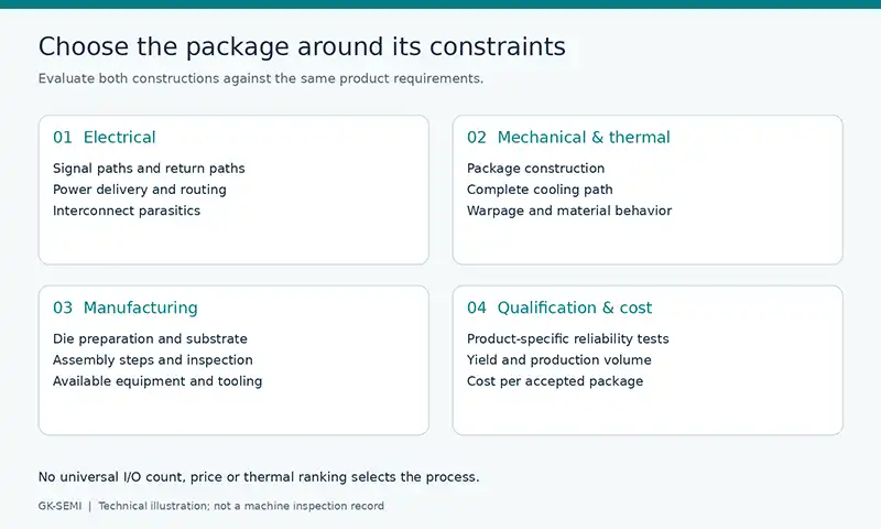
Figure 2. Compare package options against the same product requirements before selecting an assembly process.
A Practical Selection Sequence
Start with constraints that cannot easily change.
If the die is available only with wire-bond pads, a flip-chip conversion may require additional development. If dense interconnect routing is essential, a wire-bond alternative may require a larger or substantially different package.
Then compare the remaining options through electrical analysis, thermal design, assembly trials and qualification planning.
When we review bonding equipment requirements, the useful starting information is the die layout, interconnect structure, substrate, bonding process and production target. These details help establish the equipment and supporting processes required.
Frequently Asked Questions
Is flip chip the same as BGA?
No. Flip chip describes the connection between the die and its receiving substrate. BGA describes an external package connection format. A BGA package can contain a wire-bonded or flip-chip die.
Can a wire-bond die be converted directly to flip chip?
Not automatically. Pad metallurgy, bumping, layout, substrate design and package qualification must be evaluated.
Does flip chip always need underfill?
Underfill requirements depend on package construction, materials and reliability targets. Confirm the qualified assembly flow.
Can one package contain both technologies?
Yes. Hybrid and stacked constructions can combine flip-chip and wire-bond interconnects.
What should be decided before buying bonding equipment?
Define the assembly process, die and substrate formats, materials, alignment requirements, temperature and force requirements, handling method and acceptance criteria.