A bare semiconductor die fresh off the wafer has no leads, no package, and no way to connect to anything. Turning it into a functional device requires two separate operations that are often lumped together in casual conversation but could hardly be more different in purpose. Die bonding plants the chip on its carrier. Wire bonding runs the electrical connections from the chip's surface to the outside world. One operation is finished before the other begins, and neither can cover for the other's shortcomings.
Where the Confusion Comes From
Both processes happen inside the same packaging line, often within meters of each other. Both involve precise placement and thermal energy. Both are invisible in the finished product. That surface similarity leads many people to treat them as variations of the same step. They are not.
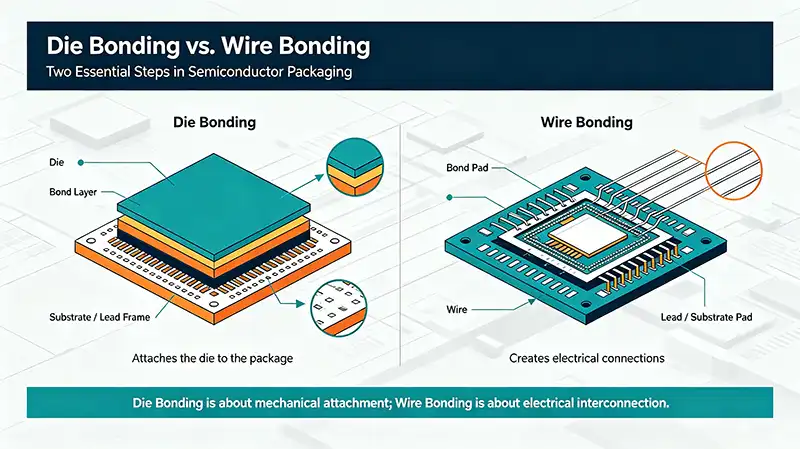
The simplest way to keep them apart: die bonding is about position and heat. Wire bonding is about current and signal.
Die Bonding: Making the Chip Stay Put
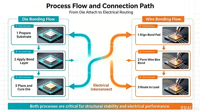
Die bonding, sometimes called die attach, begins with a pick-and-place motion. A vacuum nozzle lifts a singulated die from the wafer film. A vision system aligns the die to a target location on the lead frame or substrate. The nozzle lowers and presses the die into a measured amount of adhesive or onto a heated metallized surface.
What holds the die in place afterward depends on the material chosen.
Silver-filled epoxy remains the workhorse for most consumer and industrial chips. It cures at moderate temperatures, tolerates high-speed dispensing, and conducts both heat and electricity well enough for mainstream applications.
Eutectic bonding takes a different route. Gold-silicon or gold-tin systems form an alloy joint at temperatures above 280°C. The resulting bond has thermal resistance several times lower than epoxy, which is why power transistors, laser diodes, and high-output LEDs use it despite the higher cost and tighter process windows.
Sintered silver has gained ground in recent years for silicon carbide and gallium nitride devices. Silver particles fuse into a porous but highly conductive layer at temperatures far below silver's melting point. The joint survives temperatures that would destroy solder, making it attractive for under-hood electronics and industrial motor drives.
The die attach layer is typically only a few micrometers to a few tens of micrometers thick. Thin as it is, this layer sits directly in the primary heat path. Every void, every delaminated patch, every crack adds thermal resistance. A die attach layer with 50% voiding can push junction temperature tens of degrees higher than a void-free joint under identical electrical load. No amount of clever wire bonding downstream will fix that.
Wire Bonding: Building the Electrical Bridge
Once the die is fixed, wire bonding takes over. The goal here is to connect the aluminum pads on the chip's top surface to the corresponding terminals on the package or substrate.
Gold wire remains the default for most fine-pitch work. A spark melts the wire tip into a small ball, which is then pressed onto the die pad while the pad is heated and ultrasonic energy is applied. The gold and aluminum atoms diffuse into each other at the interface, forming an intermetallic bond. The capillary then sweeps the wire to the package terminal, makes a second bond, and snaps the wire free.
Copper wire has displaced gold in many cost-sensitive, high-volume products. Copper conducts heat and electricity better than gold and costs a fraction as much. The tradeoff is hardness. Copper requires more bonding force, which can crack sensitive pad structures, and it oxidizes readily, so the bonding environment must exclude oxygen.
Aluminum wire serves power devices and high-frequency circuits. It cannot be formed into a ball reliably, so wedge bonding is used instead: the wire is pressed flat onto the pad under force and ultrasonic vibration, creating a broad, low-profile joint. Wedge bonds tolerate higher currents and sit closer to the die surface than ball bonds.
The wire itself is fragile by design. Diameters range from 15 µm for fine-pitch signal lines to 76 µm or more for power interconnects. A human hair is roughly 70 µm wide. These filaments carry the entire electrical life of the device while enduring thermal cycling that repeatedly expands and contracts them against the pads they sit on.
The Differences That Matter
| Aspect | Die Bonding | Wire Bonding |
|---|---|---|
| Purpose | Fix the die in position; conduct heat away | Carry current and signal from die to package |
| Order in the line | First | Second, after die bonding |
| Typical failure | Delamination, void growth, thermal runaway | Bond lift, neck crack, heel fracture |
| What happens when it fails | Chip overheats or detaches | Circuit opens; device goes dead |
| Heat's role | Primary heat exit path | Negligible heat removal |
The table captures the essentials, but a few points deserve expansion.
Die bonding failures tend to be gradual. A void that forms during curing may not cause immediate problems. Over hundreds or thousands of thermal cycles, that void grows, merges with neighbors, and steadily chokes off the heat path. The device doesn't die suddenly. It runs hotter, ages faster, and eventually crosses a threshold.
Wire bonding failures are often abrupt. A neck crack that propagates through a ball bond's narrowest cross-section severs the connection in an instant. A heel crack on a wedge bond does the same. The device works one moment and fails the next.
This difference shapes how reliability testing is designed. Die attach quality is assessed through thermal cycling, power cycling, and die shear tests that measure how much force the bond can withstand before the die slides off. Wire bond quality is assessed through pull tests and ball shear tests that measure the strength of individual bonds, plus high-temperature storage to accelerate intermetallic growth.
Why the Sequence Cannot Be Reversed
The die bonder places the chip. The wire bonder finds the chip. That order is not a preference. It is a physical requirement.
Wire bonders use pattern recognition to locate die pads. If the die is not fixed, it shifts under the bonding force, and the vision system loses its reference. Even a few micrometers of movement during bonding is enough to cause a miss.
Die placement accuracy also sets the ceiling for wire bond quality. A die placed off-center forces the wire bonder to span a longer distance to reach the package terminal. Longer wires sag more, resonate at lower frequencies, and are more prone to sweep during molding. In extreme cases, the offset exceeds the bonder's recognition range and the machine simply cannot find the pads.
Thermal Reality: Die Attach Sets the Limit
Power electronics engineers spend considerable effort selecting die attach materials and minimizing void content. They spend far less time worrying about wire bond thermal performance, and for good reason.
The die attach layer covers the entire backside of the chip. Heat spreads from the junction across the full die area and passes through this broad interface into the substrate. Wire bonds, by contrast, contact the chip only at small pads. Their total cross-sectional area is a tiny fraction of the die attach area. The heat they carry is correspondingly tiny.
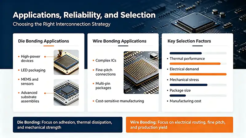
This means a device with excellent wire bonds and poor die attach will still run hot. A device with mediocre wire bonds and excellent die attach will run cool—until a wire bond cracks and the circuit opens. The two processes govern different failure timelines: die attach controls how long the device stays within thermal limits, wire bonding controls how long the electrical path remains intact.
Practical Implications for Failure Analysis
When a packaged device comes back from the field, the failure signature points to the responsible process.
Overheating, degraded performance over time, or a chip that has physically separated from its substrate points to die bonding. The attach layer has likely delaminated or voided, and the thermal path has degraded.
A device that simply stops working—no signal, no current, open circuit—points to wire bonding. One or more bonds have failed, and the electrical path is broken.
Confusing the two leads to wasted effort. Replacing wire bond parameters will not fix a delaminated die attach. Reflowing the die attach will not repair a cracked wire bond neck. The failure mode tells you which process to investigate.
What This Means for Package Design
Designers who understand the division of labor between these two steps make better tradeoffs.
If thermal management is the bottleneck, the die attach material and void control deserve the most attention. Upgrading from epoxy to sintered silver or eutectic solder can cut thermal resistance dramatically.
If electrical performance or high-frequency behavior is the constraint, wire bond length, loop height, and material selection move to the forefront. Shorter, lower loops reduce inductance and crosstalk.
If reliability under thermal cycling is the concern, both processes matter, but they fail on different timescales. Die attach degradation tends to be gradual and predictable. Wire bond failure can be sudden and catastrophic. Design margins must account for both patterns.
Frequently Asked Questions
Can a chip function without die bonding?
No. The die must be mechanically fixed before any electrical connection can be made. Without die bonding, the chip would move during wire bonding, making accurate pad location impossible. Die bonding also provides the primary path for heat to leave the chip.
Is wire bonding always required after die bonding?
Not always. Flip-chip packaging places the die face-down, so the bumps on the die surface make direct contact with the substrate pads. This eliminates wire bonding entirely. The die bonding step in flip-chip, however, must simultaneously provide mechanical fixation and electrical connection, which places much tighter demands on placement accuracy.
Which process has a greater impact on device lifespan?
Both affect lifespan, but through different mechanisms. Poor die bonding leads to elevated junction temperatures, which accelerates nearly every known semiconductor degradation mechanism. Poor wire bonding leads to open circuits, which end device life immediately. In practice, wire bond failures are more common in field returns, but die attach degradation often sets the conditions that accelerate wire bond fatigue.
Why does copper wire require more careful process control than gold wire?
Copper is harder than gold, so it needs higher bonding force. That force can crack fragile pad structures or the underlying dielectric layers. Copper also oxidizes quickly, so the bonding atmosphere must be controlled to prevent oxide formation on the wire surface. Gold does not have these problems, which is why it remains preferred for delicate or high-reliability devices.
How does die attach voiding affect thermal resistance?
Voids replace thermally conductive material with air or vacuum, both of which are excellent thermal insulators. Small, scattered voids increase thermal resistance roughly in proportion to their volume fraction. Large, contiguous voids under the active area of the chip create hot spots that can exceed safe junction temperatures even when average thermal resistance looks acceptable on paper.